Because of the Thanksgiving holiday in the U.S., TI E2E™ design support forum responses may be delayed from November 25 through December 2. Thank you for your patience.

This thread has been locked.

If you have a related question, please click the "Ask a related question" button in the top right corner. The newly created question will be automatically linked to this question.

SN74CBT3125C: Operation deficiency at 3.3V

Part Number: SN74CBT3125C
Other Parts Discussed in Thread: TMUX1511

Hello,

It seems I've made a mistake by powering the SN74CBT3125C with a 3.3V supply in my design. It's been working so far, but what operating parameters are limited at lower VDD?

The application is a 350kHz I2C bus for an external port.

  • Ch 1:  SDA 
  • Ch 2:  SCL
  • Ch 3:  not used
  • Ch 4:  VCC to load device, <1mA

All signals are the same voltage as the SN74CBT3125C supply voltage (3.3V).

Thanks

  • At 3.3 V, the on-resistance is likely to be higher.

    A FET does not allow current to pass when the voltage is near its gate voltage. This is no problem for open-drain I²C signals, but there is probably a voltage drop on channel 4. Use an analog switch that works at 3.3 V.

  • Hi Bryan,

    The SN74CBTXXXX signal switch architecture is a single NMOS FET switch.  The Vcc pin is biasing the gate of the FET and the I/O path is connected to the drain and the source.  As the voltage on the source of the FET increases and approaches the gate voltage the difference between the gate and source Vgs decreases.  As the Vgs decreases and approaches the FET threshold voltage Vt the on-state resitance between the drain and source Rdson will exponentially increase as the FET turns off Vgs<Vt.  This large on state resistance between the drain and the source can cause ~ 1V drop across the FET. 

    To fix this you can increase your Vcc which will increase the bias voltage on the gate of the FET and increase your Vgs which will keep the FET on and continue to have low on-state resistance. 

    You can also use a different device in our portfolio that has a transmission gate architecture nmos in parallel with pmos or an NMOS FET with a charge pump boosting the gate voltage.  These architectures will give you a flat resistance across the entire I/O range versus just the NMOS architecture.  These application notes goes into more detail about the trade offs between the different switch families and architectures. 

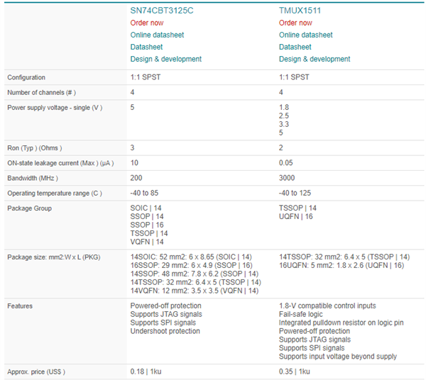
    I would like to recommended replacing SN74CBT3125C with TMUX1511, a newer part with improved parameters (Ron, ON-state leakage current, bandwidth) and more features, such as 1.8V logic compatibility, fail-safe logic, and supports input voltage beyond supply. Check out the comparison table below:

    Thanks

    Saminah