This thread has been locked.

If you have a related question, please click the "Ask a related question" button in the top right corner. The newly created question will be automatically linked to this question.

TS5A3159A: Excessive Supply Current

Part Number: TS5A3159A
Other Parts Discussed in Thread: TS5A3159, , TMUX1102, SN74LVC1T45

I am using the TS5A3159 as a switch to test battery voltage and found that the device is drawing excessive current. Please see the attached schematic showing the application.

My understanding is that the device could be operated from a 3 to 4.5v V+ voltage and that the current would be less than 500namp. In my application using 3 AA batteries the device is drawing  ~600uamp.

I cut the device out of my circuit and the total current dropped from ~630uamp to ~30uamp. I then tested the current required by the device and found the following:

3.4V ~ 0uamp, 3.6v ~0uamp, 4.0v ~35uamp, 4.2v ~ 150uamp, 4.5v ~600uamp, 4.7v ~990uamp.

The switch works perfectly as a Battery Test Switch in this circuit, but it cannot be used if it is going to drain the battery.

Please help me understand if I have made a mistake in understanding the device specification. Thanks for your support.

  • These currents looks as if there is a diode from the battery voltage to 3.3 V.

    The only nearby 3.3 V voltage is the BVM_EN signal, but the IN pin is a high-impedance CMOS input.

    Can you check whether the current flows into V+ or into COM? Does the current flow out of IN or out of GND?

    Was this tested with more than one device/board? Might there be any solder bridges? Is the chip actually a TS5A3159, and is the footprint correct?

  • Hi Larry,

    As Clemens mentioned, could you check the current at the IN, COM, and Supply pins so I can see what current is being pulled where. I think there might be multiple places current is being source from, or possibly a solder-bridge somewhere on the board. It does seem like the supply current is too high in this application. Also how many failures have you had, or is it just the one board?

    That being said it seems there is a misprint in the datasheet, supply currents are in nA for the tables, but they are in uA for the graphs, so I am going to confirm this with our test and validation team to see which range is the correct one and get back to you. It still seems you are pulling too much current but, it may be higher than the nA range as well.

    Best,

    Parker Dodson

  • I am having the same issue on other boards and another design that uses this same circuit for measuring battery voltage.

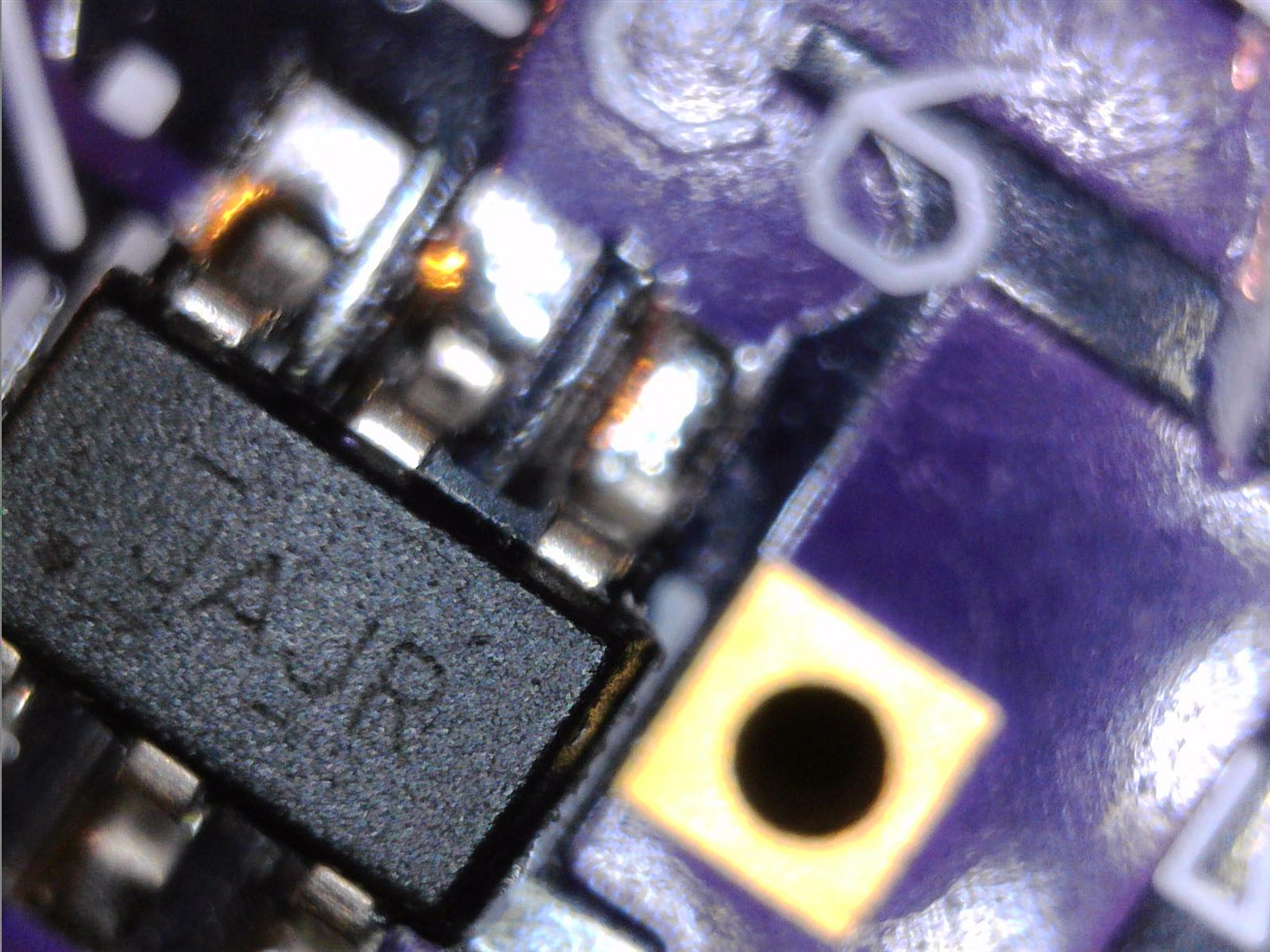
    I have attached the PCB layout showing the connections and a micro photo showing the actual device - all look OK to me.

    As you can see from the layout it will not be easy for me to separate V+ from the COM connection, but I will try.

    Thanks for replying quickly.

    Larry JohnsonTS5A3159A Power Issue Layout.pdf

  • I was able to cut the COM pin (pin 4) from V+ (pin 5). With COM (pin 4) open the same excess current flows through V+.

    As the V+ input voltage goes up, so does the excess current, these test were done with the TS5A3159 connected to all other circuits.

    So these measurements include all ICs, there may be some small increase above the original 18uamps, but most is caused by the TS5A3159A.

    3.7v I = ~18uamp

    3.9v I = ~ 21uamp

    4.0v I = ~ 46uamp

    4.1v I = ~ 92uamp

    4.2v I = ~ 172uamp

    4.3v I = ~ 309uamp

    4.4v I = ~ 470uamp

    4.5v I = ~ 620uamp

    4.6v I = ~ 822uamp

    4.7v I = ~1035uamp

  • Hi Larry,

    Thanks for checking that for me. I am talking to our team internally because I am not 100% sure on what is going on. Its pretty common for the supply to source more current as the voltage on the select line gets closer to "Input High" Threshold, so that could possibly be why you start seeing more supply current, but we didn't spec this part in a way in which we show that comparison.  When I have a more solid answer, or some more suggestions I will come back. I hope to have some answers by either the EOD or early tomorrow if I am still waiting.


    Best,

    Parker Dodson

  • Thanks Parker for your help,

    If it turns out that I made a poor choice selecting the TS5A3159A, ask if there is a better switch to use for this application.

    This is probably asking to much, but consider discussing if a new IC that measures battery voltage under a small load with voltage divided output would make sense for future development at TI.

    Take care,

    Larry Johnson

  • Hi Larry,

    There are other options, I'd suggest first looking into some 1:1 switches possibly.

    What are the reasons you originally implemented the TS5A3159A? What spec's are your key care abouts for this application.

    We have a lot of different switches that could fit this application so I want to help pin down what part will be the best fit.

    Best,

    Parker Dodson

  • Hello Parker,

    In the past I had used the TS5A3159A as an analog switch to add ADC channels, This was with V+ = 3.3v and the switch worked great.

    I had been using a NPN-PNP transistor combination with the 3K/1K voltage divider in the past to do the battery measurement. This circuit used <1 uamp when not enabled, but it took more PCB space and was not as accurate due to VCEsat offset when making the measurement.

    I looked at the TS5A3159A switch and saw no reason it could not be used as a replacement to make this measurement (the Iq spec of <500namp looked good). I did not see an indication that the switch current would increase when V+ increased from 3.3v to 5v and the accuracy would be much better than the transistor circuit. I also had looked at using load switches, but they increase the time needed to make the measurement.

    I assume from your email that the TS5A3159A cannot be used at 5v without the increase in Iq current. 

    I will look at other TI analog switches, but I will need some assurance that they will work in this application.

    Take care,

    Larry

  • Hello Parker,

    I have looked at all the TI switches and now believe I understand why the current is larger than I originally thought.

    For each of the TI switches the "Iq" value is specified when VIN is either at Gnd or V+. So none of the TI switches will have low "Iq" with VCC operated at greater than 3.3v and with VIN = 3.3v. 

    I did find a "work-around" by switching the default VIN to the TS5A3159A to logic "0" when the battery is not being tested. Then using VIN 3.3v when the battery is tested, the extra 600uamp will not be a problem for this short period of time. I was lucky that I have a SPDT switch instead of a SPST switch so the PCB change is small.  It is amazing to me that with VIN = 0v that the current drops to almost 0. Will there be a reliability issue with VIN = 3.3v during the battery measurement time?

    Regards,

    Larry

  • VIH is 2.4 V, so it is guaranteed to work with a 3.3 V signal.

    Switches like the TMUX1102 have 1.8-V compatible logic inputs, i.e., a 3.3 V signal will not have cross currents.

    Alternatively, put a level shifter (e.g., SN74LVC1T45) in front of the input.

  • Hi Larry,

    No as Clemens mentioned, the VIH is 2.4V so there shouldn't be a reliability issue during battery measurement time. As long as you can handle the turn_on/turn_off time of the device, which is has a max of 50ns either way, depending on the VDD voltage. 

    Best,

    Parker Dodson