This thread has been locked.

If you have a related question, please click the "Ask a related question" button in the top right corner. The newly created question will be automatically linked to this question.

TS5A3159: TS5A3159MDBVREP Digital Input transient withstand capability

Part Number: TS5A3159

Hello,

We are using the device TS5A3159MDBVREP for one of our application.

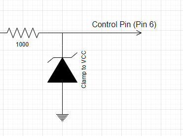
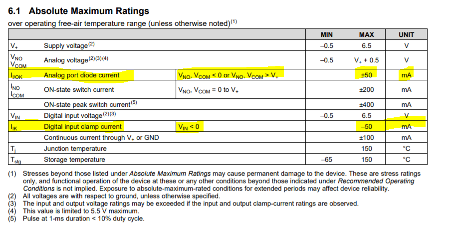
For the digital control input pin no 6 of the device there is a transient with the following spec.

While switching from 0 to 5V at 3KHz rate,

Peak Overshoot : 7.26V.

Peak Duration : 20nS

While switching from 5V to 0, 

Peak Overshoot : -2V.

Peak Duration : 20nS

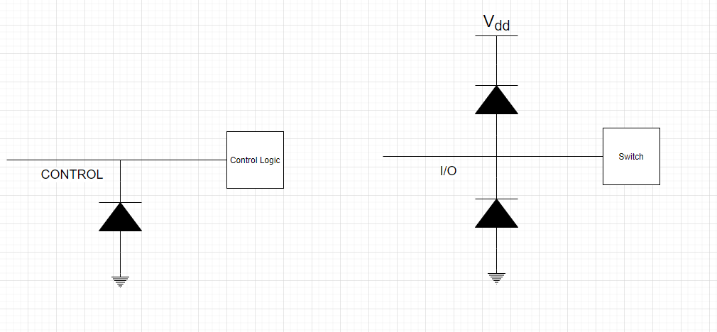
Refer attached images.

Kindly tell us the impact of this input signal transient on the reliability performance of the switch.

I cannot remove this transient from my actual test setup, does providing this transient damage the IC during long run or we can ignore this transient.

Does this clamping diodes will suppress this transient?

  • Hi Sai,

    It could cause problems/damage. Both the overshoot and undershoot are out of spec and have the ability to cause damage. 

    However the main concern is current that will be conducted through the ESD clamping diodes during these events. There are 2 possible scenarios:

    1. The the current going in / out of pin 6 during the transients  have a peak <50mA. In this case the application shouldn't have issues as the clamping diodes can handle the spikes.

    2. Current going in/ out of pin 6 during transients exceeds 50mA. In this case a current limiting resistor needs to be added to ensure that the ESD diodes do not become damaged and destroy the IC. The resistor size just needs to keep current going in/ coming out of pin 6 to < 50mA during those transient events.

    If you have any other questions please let me know!

    Best,

    Parker Dodson

  • Hi Parker,

    Thanks for the reply.

    Yes I am having the series resistor of 1 k ohms to the pin 6, I hope this transient will not have have any impact on the long term reliability of the IC, am I correct ?

    Regards

     Sai Kiran S.

  • Hi Sai,

    I apologize - I made a slight mistake.

    On the Control pin (Pin 6) there is only a clamping diode to ground. This means that this pin will not clamp down to VCC if an overvoltage event occurs.

    That being said - the solution is to use a clamping diode that will clamp the line to ideally VCC - but it can go up to 6.5V on that pin without sustaining damage. That being said the 1k Ohm resistor will work for the undershoot - but for the overshoot a clamping diode also should be added. I have added a diagram showing this below:

    This will help prevent damage to the IC due to the transients you see at switching.

    If you have any other questions please let me know!

    Best,

    Parker S. Dodson

  • Hi Parker,

    Can you share me the clamping diode scheme diagram provided on the input pins of the IC for my better understanding.

    Regards,

    Sai Kiran S

  • Hi Sai,

    The clamping diodes within the device are there for ESD strikes so they aren't great at clamping - i.e. the small amount of current they can handle.

    That being said the ESD structure is simple and can be deduced using the abs max table - below is the two structures found in this device:

    This means that the control pins can't be over-volted because there is nothing to clamp it to VDD. You can tell this from the abs max table - which I have included below:

    First you can look at the highlighted part - the digital port clamping diodes can only source current - it can't sink this means the ESD clamps are between the pin and ground. While the analog port clamping diodes can source or sink current meaning there is diodes to ground and VDD.

    You can also look at the voltage ratings. 

    For I/O the min is -0.5V below ground (this is the point that the clamping diodes can be burned up due to excess current) this is the same for the digital input voltage min at -0.5V below ground - because they both have clamping diodes to ground. However when you look at max voltages - analog input is (V+) + 0.5V and the digital input is 6.5V. This means there is no clamp to VDD on the digital pin because it isn't value + diode drop it is a singular value. That is why a zener clamp on the control pin can be used to keep the digital voltage to within VDD's levels (+ some margin).

    If that wasn't clear or you have any questions please let me know!

    Best,

    Parker Dodson

  • Hi Parker,

    As you said the clamp diode to ground which is present on the control pin IC also not responding to the transient for 20nS duration.

    I may have to see any bi directional TVS or ESD which will respond to this transient voltage, If not I will try to control at source end only.

    Regards,

    Sai Kiran S