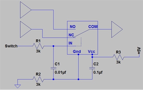
Someone tell me what is wrong with a scheme I devised to nullify the Con of an analog mux (single, 6-8 pin part such as TS5A94411 or TS5A2053).
In my application the capacitance of the analog mux is affecting the frequency response of my signal above 100MHz. It occurred to me that I might put a 3K resistor in series with the Vcc, Gnd and the control input and then a bypass cap between Vcc-Gnd and Cntr-Gnd. I would also clear any copper from below the part.
It seems to me that the signal would now see at least 1k ohms in series with the Con and thus Con would not affect my signal.
The isolation spec implies that the channel to channel capacitance is less than 1pf. The part only draws 1uA of supply current. I might need to add a 5V zener across Vcc-Gnd to account for effects of charge pumping through the protection diodes but if the bypass cap is large relative to Con I don't think I will.
I can't find the flaw in this scheme; but, it seems too easy.


