For more answers to your questions, check out the new FAQ page!
This page features a growing list of similar and frequent questions asked about TI's multiplexers and signal switches.
I don't know what a specific parameter, characteristic, or feature in the datasheet means. Where can I learn more?
Take a look at the Multiplexers and Signal Switches Glossary. This document serves as a reference guide for datasheet parameters/characteristics and definitions of common terms and features.
For more detailed answers on key characteristics, features, and FAQs, find our TI Precision Labs video series here.
How do I select a specific device for my application?
This document, Selecting the Right Texas Instruments Signal Switch, provides detailed information about TI's portfolio of analog switches/muxes.
To search for the device you need, use the Analog switches/suxes product search tool. Here you can filter and sort by configuration, channels, and parameters to fit your system requirements.
Can the voltage on the I/O pins of a switch be greater than VCC or less than 0 V?
-It depends on thje Absolute Maximum Ratings table.
Sometimes the input will have a limit of "-0.5 V (min) to VCC + 0.5 V (max)," which means that there is a forward-conducting ESD diode from the input back to VCC and from the input to ground. In this case, an input higher than VCC or lower than 0V is not allowed unless there is a series resistor limiting the current into the input to less than the IIK or IOK maximum clamp current rating.
-If the input has a limit of, for example, "-0.5 to 7 V," then the maximum voltage is not dependent on VCC, there is no diode to VCC, and the input is overvoltage-tolerant, allowing you to have inputs greater than VCC. However, inputs greater than VCC will not pass through unattenuated on most switches.
What is the maximum signal rate or data rate of a signal switch?
-The best way to figure out the maximum signal rate or data rate is to estimate based on bandwidth. TI specifies switch bandwidth as the point where the output is attenuated -3 dB from the standard DC attenuation. On most switches, there is a bandwidth curve in the datasheet or in an application report.
To calculate the maximum data rate the bandwidth can support you can use the theoretical formula DataRate = 2xBandwidth.
In practice we recommend selecting switches with more bandwidth than what is theoretically required for a particular data rate to account for system losses that occur on PCB traces etc. The rough formula we use to select switches is Bandwidth = (3/2)xDataRate which will provide sufficient margin.
Are TI analog/digital switches/multiplexers bidirectional?
-Yes, all analog and digital bus switches are bidirectional. View this brief training video, Are switches & multiplexers bidirectional?, for more information!
This means that the switches do not have their body terminal tied to any one terminal, which means the drain and source terminal are interchangeable depending on where you are applying your signal. Please see the diagram below on what a FET switch looks like on the silicon level:
How to calculate the maximum junction temperature and power dissipation for a signal switch?
You can use this excel calculator to calculate the max power dissipation as well as the maximum junction temperature. 0486.Signal Switch power dissipation and junction temperature calculator.xlsx
You can also reference this post for more information on the calculation.

May I use a differential switch for a single ended application?
TI's differential switches are high performance devices designed to have excellent channel matching which is a key requirement for most differential signaling applications. You may use these differential switches in single ended applications.
What is the switching time of my device?
An overview of timing characteristics may be found in the Multiplexers and Signal Switches Glossary.
For more information on each timing characteristic, check out this TI Precision Labs video.
- Turn-on time (ton) and Turn-off time (toff): Turn on time is the time required for the signal path to change to the ON state as a response to the enable pin ON trigger. Turn off time is the time required for the signal path to change to the OFF state as a response to the enable pin OFF trigger.
- Propagation delay (tpd): The time required for a signal to pass from the input signal pin to the respected output signal pin.
- Transition time (tTRAN): The time required for the switch output to settle to the expected value or change signal paths due to a change of the digital input (SEL) pin.
- Break-before-make delay (tBBM): The time delay to ensure that the current on-state signal path is disconnected before the next on-state signal path is connected.
Can I leave unused pins floating?
This training video answers this question for all potentially unused pins of a device: signal pins, control pins, VSS, No Connect pins, and thermal pads.
- Switch control inputs must always have a defined state. If the device does not have internal pullup or pulldown resistors, the pin must be tied to a known voltage.
- Switch signal input/output pins may be left floating. In high speed applications, best practice is to terminate these unused pins to GND.
What is the difference between an analog switch and a digital bus switch?
Check out this training video, What are common switch architectures?, to learn more about the architecture of analog and digital switches!
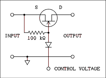
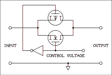
TI's analog and digital bus switches are electrically equivalent and both share the common switch architectures found in the semiconductor industry.
Single FET switch
Bilateral FET switch
for more information about these switch architectures see this app note, "Selecting the right Texas Instruments Signal Switch."
Even thought the different ICs have the same electrical structures, the terms "analog switch" and "digital bus switch" were introduced to help TI categorize its large switch portfolio into 2 different groups, high channel count switches and low channel count switches.
Typically you will find the high channel count switches in the portfolio labeled "digital bus switches" because digital buses usually have many more signal paths than analog signal paths for their common use of transmitting 8, 16, 32 bits of data. As TI's switch portfolio continues to expand this loose distinction between analog and digital devices are becoming irrelevant.
What are VIH and VIL? Is my control signal compatible with my mux's input logic levels? Do I need a mux with 1.8-V compatible control inputs?
This training video, Output/Input logic levels (VOH, VOL, VIH, VIL), discusses the definition of the input and output logic levels. Learn how to ensure your control signal is compatible with the input thresholds of your mux.
1.8-V compatible muxes and switches simplify design of systems with multiple power rails. 1.8V logic muxes eliminate need for external logic level translation.
Where can I learn more about switch "features"? How do I know which features I need?
More and more switches are offering features to further protect your devices and system from damage and malfunctions. The following TI Precision labs videos offer in-depth explanations of the benefits of each feature:
- Simplify power sequencing with powered-off protection
- What is overvoltage protection?
- What is fail-safe logic?
- Preventing crosstalk with injection current control
- What is latch-up immunity?
Where does the exposed center pad for RGY and RGT packages connected to?
It is suggested to soldered the exposed center pad to the PCB for thermal and mechanical performance. The pad may be electrically connected to ground. Please refer to the datasheet mechanical information for detailed information and could refer to the app note here .
Signal switch naming convention and vocabulary
Does TI have any Normally Closed switches when Vcc = 0V ?
TI's signal switches are solid state switches but they steal the naming conventions from mechanical switches. The terms Normally Closed (NC) and Normally Open (NO) describe the normal (unenergized) physical position of the mechanical switch. The figure below shows that the 1-3 path as normally closed and the 3-2 path is the path that connects when the conducting wire physically moves to connect the 2-3 path.
Unlike mechanical switches, solid state switches do not have any moving parts internal to the IC. Technically the Normally Closed (NC) path and (NO) are always physically connected inside TI's signal switches. To turn "ON" the switch or connect the signal path from one side to the other requires a bias voltage to the gate to allow current to flow between the drain and the source.
Solid state switches that conduct with out a bias voltage applied to the power supply Vcc utilize depletion FETs which will conduct without a bias voltage and isolate when biased. Currently TI does not offer a signal switch with depletion FETs to create a "normally closed" solid state switch. If you need this type of device we would be happy to talk about creating this type of device and how using depletion FET switch fits into your system.
What is On/Off Leakage?
Off leakage is when you turn off the switch and there is still a parasitic current which bleeds through the switch onto the output. This physical phenomenon that occurs is because a switch is not a perfect signal block when turned off. It behaves very closely to one, but if you view the image of a NMOS, you can see that although there is no voltage applied to the gate, you can still have charge slip through to the other side. Problems that come from this is your device is offset voltage sensitive, you will begin to see a change in voltage on the other side of your MUXed application depending on the load resistance. An image of how we test for off leakage can be seen below:
On leakage, however, is the when there is additional current that appears on the output or is sources from the input. This phenomenon happens due to the parasitics of the device mentioned above. These parasitics will draw current into other portions of the device, and likewise other portions will leak charge into the output of the device. The same problem can occur as that of the Off state leakage, which makes using sensitive sensors tricky. Please see below for the the On-state switch leakage current:


