This thread has been locked.

If you have a related question, please click the "Ask a related question" button in the top right corner. The newly created question will be automatically linked to this question.

SN74LV4051A: channel switching delay

Part Number: SN74LV4051A

Hi,

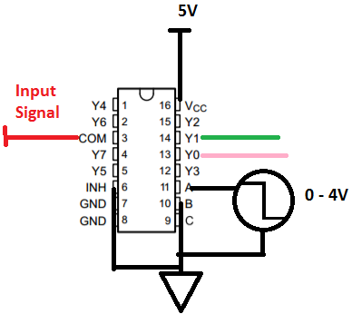
Please tell me about channel switching delay time of SN74LV4051A.
Can anyone please let me know whether this part SN74LV4051A can support this switching speed
from one channel to next channel without any disturbances in applied voltage at the 8 analog channels.

For example:

I would like to know the delay time of Y2 to Y4 when A, B, and C are controlled with INH=L fixed.

best regards

  • Cafain,

    I took a look at the SN74LV4051A datasheet to see the delay when switching between channels. As you probably already found out the information was not in datasheet. This is an older device and I will need to see if I can track down this data in some legacy archives. I will also check in on ordering this device and some hardware to test it in the lab.

    What are you doing in your application that it is sensitive to the switching time? What is your target for this spec?

    Thank you,
    Adam
  • Hi, adam-san

    I do not want to disclose the application, so do you offline?

    cafain

  • Sure, I will send you a friend request to protection your confidential information.
  • Hello Cafain,

    I did some tests on the SN74LV4051A for the delay between switching channels.  The general test setup can be observed in Figure 1.  For these tests, the input signal on the COM pin was just a constant voltage.  In these tests the switching delay between channels Y0 and Y1 was assesed.  Only these channels were assessed as we expect similar performance from the other channels in this particular device.  Channel 1 (yellow) corresponds to the signal inputted at pin A to switch between channels Y0 and Y1, while channel 3 (magenta) corresponds to Y0 and channel 4 (green) corresponds to Y1. Figure 2 shows the delay observed when switching from channel Y0 to Y1 and this is ~19.6ns.  Figures 3  and 4 show the delays for switching from Y1 to Y0.  The maximum delay observed for this switch was  ~12.4ns.

    Figure 1

    Figure 2

    Figure 3

    Figure 4

  • Hi, patrick san

    I thank you very much for having detailed explanations and experiments.
    It is an answer that matches the problem I requested.

    When the COM terminal input is fixed and the channel switching signal (A, B, C) is changed, the inter-channel delay time is roughly within 20ns.
    It is important data for the user.

    best regards
    cafain

  • Hello Team;

    Please let me check it.
    When all A, B, C are switched at the same time,
    Will not a voltage different from the output of the selected channel be output?
    (Do you have any case examples?)

    * Even if the channel is switched, the operation that the output voltage different from the input voltage is outputted
     because it was confirmed (reproducibility is very low)
      I am checking that this behavior is related to 4051A, so I am checking it.

    best regards
    cafain

  • Hello Cafain-san,

    In Figures 1 and 2 below are the results I get when switching A, B , and C all at the same time.  For my results there is a noticeable drop (~600mV)  from the input of COM to the output of Y0 and Y7.  This is actually expected behavior due to the particular setup I have used as shown in Figure 3.  The amount of voltage that drops across the  SN74LV4051Aswitch hinges on the termination impedance of your input supply as well as the load seen at the Y pins.  Another important factor is the parasitic Ron resistance of the internal FETs in SN74LV4051A.  Essentially these FETS, which for the purposes of simplification can be treated as resistors (Figure 4), form a voltage divider with your load and source impedances (Figure 5).  Upon looking at the Ron in the Electrical Characteristics section of the datasheet (Table 1), one can see that depending on the Vcc, temperature, and device variation, this parasitic resistance can range anywhere from less than 22 ohms to 600 ohms.  Consequently if you have a small load impedance, it is quite likely you will observe inconsistent output voltages between different units.  However, if your load is 10 to 100 times larger than Ron, you should expect to see a very negligible drop across the switch.

    Figure 1

    Figure 2

    Table1

  • Hi, Patrick-san

    Thank you for presenting accurate and fast data.

    I am concerned whether the memory effect that the capacitor capacity of the internal MOSFET will affect will not affect the 4051A switch.

    best regards

    cafain.

  • Hi, Patrick-san

    Is such confirmation possible?

    Input 3V to the Y0 terminal (DC), 0V to the Y7 terminal.
    After first setting A, B, and C to L, L, L and confirming that 3V is output to the COM terminal,
    We expect that A, B, and C terminals are set to H, H, H and 0V is output to the COM terminal.

    Despite having set it to COM - Y7, will it operate such that 3V is output to COM?
    (It is assumed that it does not work)

    best regards

  • Hello Cafain-san,

    According to the description from the datasheet, inputting the signal at Y7 and outputting at COM should not be a problem.  Also inputting the signal from Y0 and outputting at COM should not be a problem.  By setting the logic levels on pins A, B, and C, you essentially determine the signal path to or from COM.  If you observe behavior that deviates from this, please let us know.

  • Hi,Patrick-san

    I got detailed data and got to know deeply the behavior of the device.
    It helps design & support.

    best regard

    cafain