This thread has been locked.

If you have a related question, please click the "Ask a related question" button in the top right corner. The newly created question will be automatically linked to this question.

SN74LV4051A-Q1: Limiting the diode current for avoidance of device damage

Guru 16770 points
Part Number: SN74LV4051A-Q1

Hi

I'm wondering if the device would be damaged or not under the following case.

Our assume is following.
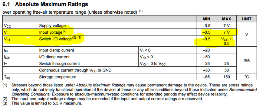
The 18V voltage is applied to Yx as the input via series 20Kohm register, and VCC is 5V.

( INPUT (18V) -> [20Kohm resistor] -> Yx pin )

The IO diode current conducted to VDD and GND would be limited by ~900uA (18V/20Kohm)  with series resister.

In this case, would the device be damaged?

What is your view?

BestRegards

  • Hello,

    For this question, I would refer to the absolute maximum ratings for the SN74LV4051-Q1:

    Although there is a subnote stating that the voltage may be exceeded, TI does not recommend doing so. At 18V, despite the current limited, there could still be damage, if not immediately, there can be damage over time due to over voltage stress on the device itself. 

    Could you tell us what is on the COM side for your application so that we can better understand this signal chain?

    Thank you, 

    Louie

    If I have answered your questions, please hit the Verify Answer button.

  • Hi Louie

    Thank you for your reply.

    And sorry, my question might have not been clear.

    We have to consider the countermeasure to avoiding device damage under particular situation.

    (This considering is required for automotive device)

    Of course, we never apply 18Vdc to input terminal in normal operation.

    So we want to know if there is possibility whether SN74LV4051A-Q1 could be damaged or not, in the following example.

    And I did simulation of our supposition. (Using Vf = 0.4V in  simulation case)

    According to this simulation, the voltage at the anode of diode (it is expected Yx terminal) is 5.4V and

    it conduct current (18V-5.4V)/20kohm = 629.7uA.

    Regarding to SN74LV4051A-Q1, it would have protection diode to VCC and GND whose Vf should be around 0.5V.

    So, I think the voltage at Yx of SN74LV4051A-Q1 would be 5.5V and the internal diode would conduct (18V-5.5V)/20kohm = 625uA.  

    These values seem to meet the datasheet ratings.  

    I have following two questions.

     Please tell us your view?

    1.

    Could the upper simulation result be possible to apply as SN74LV4051A-Q1 case?

    2.

    If not possible, it means the device could be damaged in this configuration.

    If the device had damage in this configuration, what happens to the device?

    Open? Short? or other malfunctioning?

    BestRegards

  • Hello,

    I believe your simulations are with the assumption that this part has a pull up diode for protection. Unfortunately for this part that is not the case. If you refer back to the data sheet snippet with the absolute ratings, you will note that the diode current specced is for all Vi/o's below 0V, which means there is only a protection diode between input to GND:

    In this instance, TI still would not recommend this scenario in your simulations since they are based on the assumption of a pull up diode for protection.

    If the device is damaged from over voltage stress, it is likely that the device will become open, but without lab testing, this answer is unclear. 

    Thank you,

    Louie

    If I answered your questions, please hit the Verify Answers button.

  • Hi Louie

    Thank you for your reply.

    I confirmed the pull up diode to VDD in the following thread.

    e2e.ti.com/.../540249

    Does this device have no diode between intput and VCC?
    Could you please check it out again?

    And please tell me the answer to my assumption?

    BestRegards
  • Hello,

    Thank you for sending that link, after reviewing the last two E2E posts, and consulting with my team yes there should be an ESD diode to Vcc. With the current limiting resistor, you will be protecting your diode, if the assumption is that it is as minimal a 0.5V drop across the pull up ESD diode. There are some instances, use over time for example, where this drop can increase, so please be careful because the Vinput can rise up to 5.7V, which exceeds the absolute ratings for this device.
    I would like to add in one more condition, please also ensure that your Vcc source can sink current.

    Thank you,
    Louie