This thread has been locked.

If you have a related question, please click the "Ask a related question" button in the top right corner. The newly created question will be automatically linked to this question.

SN74CBT3245A: Setting VCC for level shifting application

Part Number: SN74CBT3245A

Hello,

If we set VCC for all parts we buy to 4.2V, will this guarantee 3.3V max at the A side IO pins under all conditions? Wondering what the variation in VCC might be for each part we use to achieve the same 3.3V max on A side. +/- 0.2V, +/- 1V?

Thanks,

Nick

  • Nick,

    Let me try and rephrase your question to make sure I understand correctly.  You would like to know the variance in the FET switch Vt threshold that causes the output signal to clip relative to the input signal.  Like a statistical distribution of Vt as a result of the manufacturing process. 

    I will need to check with our design team as I believe that information is a trade secret to TI's proprietary silicon processing.  I will let you know if we can share that information.

    Why do you need to know that information in your system?  Maybe we can help you find a different parameter that we can share information.

    Thank you,

    Adam  

  • Hi Adam,

    From our setup test we saw that when Vcc was around 4.2V, the voltage at the A I/O pin hits 3.3V and FET is off. At this point our B side pulls up the rest of the way to 5V (when pulled to 5V through resistor) while the A I/O pin remains at 3.3V. We can't have the A side go above 3.3V so want to guarantee under all conditions it will max out at 3.3V. So wondering if Vcc around 4.2V on all parts used will keep A side from going above 3.3V.

    Thank you,
    Nick
  • Nick,

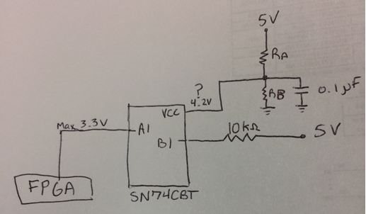
    The SN74CBTXXXX devices are passive nmos FET switches and voltages on the A/B pins of the signal path will be dictated by the system around the IC since it doesn't have any current sourcing or sinking capability. Do you have a schematic or diagram of your system around the switch?


    With Vcc set to 4.2 V and the signal path conducting, if you placed 5 V on the A or B side you will notice that the opposite side of the signal path will not make it up to 5V but somewhere around 3.3 V due to the Vt<Vgs discussed above. If the signal path is not conducting it will be Hi-Z and only a couple of micro amps will be able to leak from one side of the signal path to the other.

    Thank you,
    Adam
  • Hi Adam,

    Yes I believe that is what we want. Here is a schematic, I hope it is readable. Ideally, with Vcc = 4.2V we will have A=B until A reaches about 3.3V, at which point the FET is effectively off and the B pin should get pulled the rest of the way to 5V while A remains at 3.3V (Can't have A any higher than probably 3.4V or risk damage to FPGA). Same setup for all 8 channels. So we found that point to be at Vcc = 4.2V on the sample part we used, but we're wondering if that will be roughly the same for all parts we use. So will Vcc=4.2V guarantee 3.3V max at A I/O pins under all conditions? And will Vcc=4.2V work for all parts we use or will some parts possibly require 4.1V to guarantee a 3.3V max at A? If that variation is only +/- 0.1V then we're probably fine but if it is much more than that then we may have to rethink. 


    Thanks,

    Nick

  • Nick,

    Thank you for the additional diagram that helps clear up your need a little more.  We do not specifically guarantee the Vt voltage variation tolerance of the FET switch so I have a solution for you below how to calibrate out the Vt variation or we might want to look at a different set of devices. 

    May I suggest using SN74CB3TXXXX family or SN74CBTDXXXX family of switches for your application?  These devices are designed for the level shifting function you are looking for and can eliminate some of your additional circuitry.  I have attached some applications notes that will help provide more details. 

    Thank you,

    Adam