This thread has been locked.

If you have a related question, please click the "Ask a related question" button in the top right corner. The newly created question will be automatically linked to this question.

SN74LV4051A-Q1: internal connection from I/O pins to Vcc or GND

Guru 20090 points
Part Number: SN74LV4051A-Q1

Hello,

I would like to know the following pins internal connection to Vcc or GND.

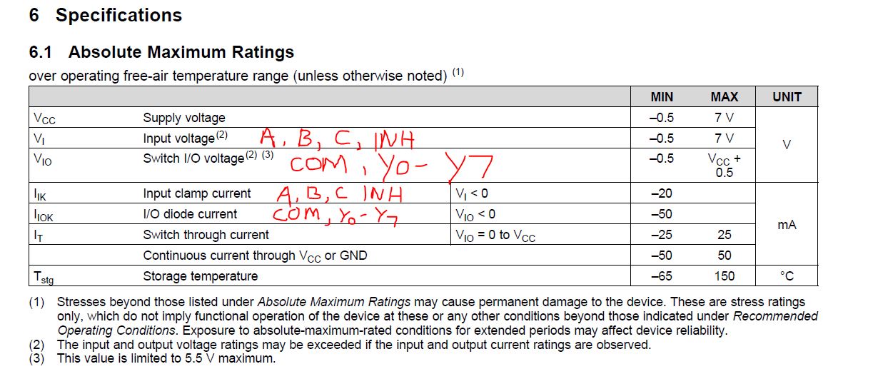
(1) Yx pins to Vcc/GND
(2) A/B/C pins to Vcc/GND
(3) COM pin to Vcc/GND
(4) INH pin to Vcc/GND


From the Absolute maximum ratings, I think that the Switch I/O pin has protection diode to Vcc/GND and Input pin does not have protection diode.
However, I couldn't understand which pins are switch I/O pins. (Yx and COM pins?)

Best Regards,
Ryuji

  • Ryuji,

    The pin description table in the datasheet states the pins with note (1) are the I/O pins which include COM and Y0-Y7.  The select pins are A, B, and C and the INH (inhibit) pin are digital logic pins to control the selection of signal path.  

    There is an error in the table below and the INH pin should not be an I/O pin with the note (1)

    You are correct based on the abs max table the I/O path has protection diodes to Vcc and Ground but the digital control logic pins only have protection diode to ground.

    Thank you,

    Adam

  • Hello Adam san,

    I appreciate your support.
    I understood.

    Best Regards,
    Ryuji