This thread has been locked.

If you have a related question, please click the "Ask a related question" button in the top right corner. The newly created question will be automatically linked to this question.

SN74LVC1G3157: Control input switching issue causing excess current consumption

Part Number: SN74LVC1G3157
Other Parts Discussed in Thread: TMUX1119

We are using SN74LVC1G3157 as analog switch in our design. Below is the configuraion of the switch.

VCC - 5V

GND - Ground

S - 32KHz signal (4V high level, 0V low level)

B2 - 2.5V

B1 - Ground

Based on the control switch frequency, B1 or B2 will be connected to A.

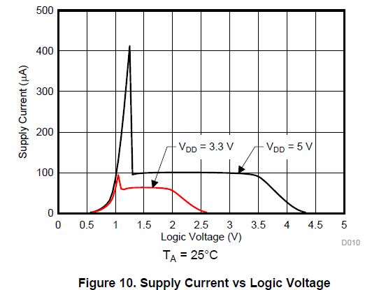
The issue with that configuration is that the device current taken from the VCC (5V) is around 12mA max when the switch input S is held high or held low for some time in between the 32KHz switching.

Please clarify this and confirm that the input frequency to S pin is acceptable or not. Since I couldn't able to find relative information for that input.

Regards

Maharajan

  • Maharajan,

    There will be excess current consumption for this device anytime the S pin voltage is not at Vcc or ground.  This is due to the shoot through current when the S pin input buffer partially turns on both the high side and low side FET of the inverter and creates a low impedance path from Vcc to ground.

    More information can be found by typing "excess current consumption" in the switches and multiplexers search bar

    One way you can avoid the excess current consumption is to have your S pin swing all the way to Vcc (5V in your case) and reduce the amount of time that the switch S pin is not at Vcc or ground.

    The frequency performance on the S pin is not characterized for this device but I don't think 32kHz is out of the ordinary for this part. 

    The new TMUX1119 device has better current consumption performance defined when the logic voltage is not at supply. 

    Thank you,

    Adam