This thread has been locked.

If you have a related question, please click the "Ask a related question" button in the top right corner. The newly created question will be automatically linked to this question.

SN74CBT3251: Failure Analyze for SN74cbt3251

Part Number: SN74CBT3251

Hi Team,

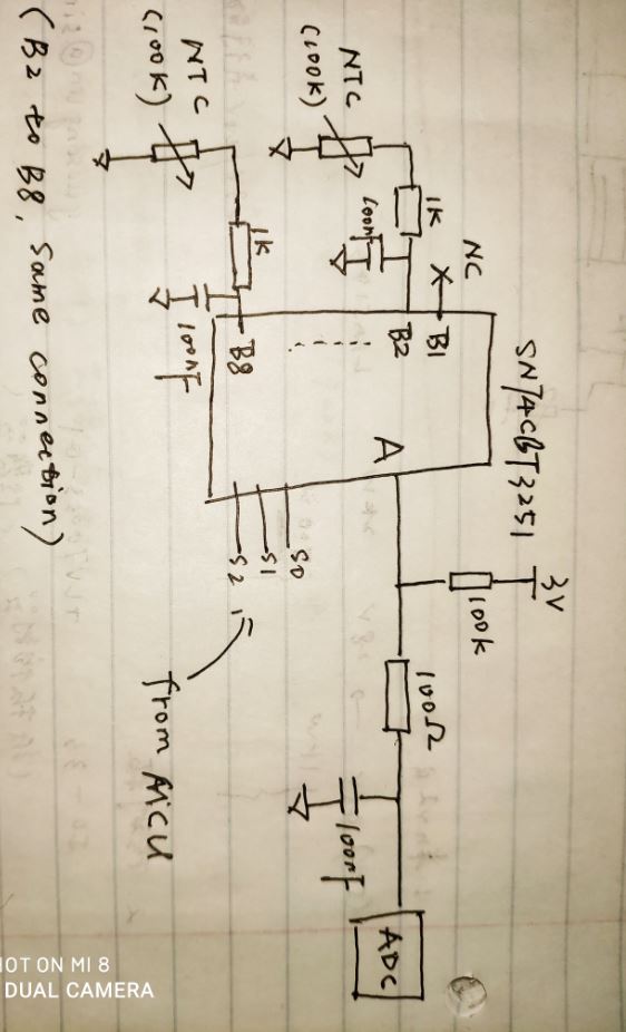
SN74CBT3251 was used in customer. The input PinB1~ B7 was shorted TO ground randomly when SN74CBT3251 was used to sample temperature.Here is the schematic for SN74CBT3251. The failure rate is 2%.

This is a special application, B1 is NC, the rest B2~B8 connect to NTC, When MCU control enable pin to open the path, NTC is pulled up by the pin A.

We also test the power sequence for this application, 5V is powered up first. Could you give us some advice? Thanks.


BR

Songzhen Guo

  • Hi Songzhen,

    To help debug, can you provide details on the following:

    • When you say failure rate of 2%, can you specify what is failing - are you not getting any output, is it not performing the switching?

    • Can you share scope capture at Inputs and output?

    • What is your input signal voltage  on B2-B8?

    • Could you also check what does the signal look like if you remove the mux and short the signal path?

    • Have you replaced the switch with new IC -What result do you see?

    Regards

    Saminah

  • Hi Saminah,

    See the update below:

    B2~B8 is not input in this application, when internal switch is close, the current is flow to B2. The voltage on A is changed.

    When you say failure rate of 2%, can you specify what is failing - are you not getting any output, is it not performing the switching?

    Failure scenario:

    B1 is NC and B1 is good all the time.

    Several Pin of B2~B8 were shorted to ground randomly,the maximum number of damages is 4.

    The switching performance is wok well.

    Can you share scope capture at Inputs and output?

    the yellow one is the input signal of B2, The output is flow the input.

    the pink one is the trigger signal of S0.

    What is your input signal voltage  on B2-B8?

    B2~B8 is not input in this application, see the picture below.

    Could you also check what does the signal look like if you remove the mux and short the signal path?

    If we remove the MUX, it's a resistor net.

    Have you replaced the switch with new IC -What result do you see?

    Yes. after change the IC,  it works well.


    BR

    Songzhen Guo

  • Hi Songzhen Guo,

    You mentioned after changing the IC, you don;t see any issue - can you check this with 2-3 other ICs and confirm if you still don't see any failure?

    Regards

    Saminah

  • Saminah,

    This is the action customer did:

    At first, take one failure board, the SN74CBT3251 is damaged;

    Then, we remove SN74CBT3251, B2 is shorted to GND;

    After that, take a new Sn74CBT3251, slot new SN74CBT3251, this SN74CBT3251 is work well

    Customer don't try several new IC. They want to know why SN74CBT3251 was damaged on board.

    Could you review this circuit for customer? I have several question for this circuit:

    Is the current flow right?

    Is SNCBT3251 a bi-direction device?

    What's the switch model in side? Is there any risk for this circuit? Can it cause voltage glitch on B2~ B8?(Because B1 is NC, and B1 no damage);

  • Hi

    I don’t see anything wrong with the application circuit and current flow looks correct

    Can you confirm the Sx logic high level and the VDD level.

    Also, check the power up/down conditions. Since this device doesn’t seem to have powered off protection or fail safe logic, we need to power VDD before the logic and the IO pins.

    All our signal switches are bi-directional. CBT switch is an NMOS series switch and Vt is the  threshold voltage of NMOS - See more details here on this switch structure in Switches and muxes: What are common switch architectures?

    You can leave B1 as NC but it is good practice to connect I/O pins to GND if they are unused so the input status is not left undetermined.

    Regards

    Saminah