This thread has been locked.

If you have a related question, please click the "Ask a related question" button in the top right corner. The newly created question will be automatically linked to this question.

SN74TVC3306: I2C level translation to very low voltage

Part Number: SN74TVC3306

Hello !

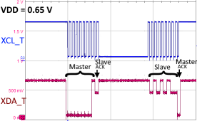
I am using the SN74TVC3306 dual-votlage clamp to interface an I2C master at 1.8 V, to an I2C slave powered down to 0.5 V. It is working correctly down to 0.7 V (on the slave side), but my slave seems to be unable to pull-down the SDA signal when the power supply is lower than 0.7 V. There is only one master and one slave on the I2C bus.

My question is :

- can I use the SN74TVC3306 down to 0.5 V voltage supply on the slave side ? If not, is there any solution in integrated or discrete form ?

Best regards,

Philippe Sauvain
R&D Engineer
SG R&D Ltd

  • Philippe,

    Is the 0.5V supply on your slave side the Vref point you're look to set your voltage translator to as the 'voltage limiting point'?
    Could you show a block diagram or schematic of your setup?

    Rami

  • Hello,

    You find below the schematics of the level shifter in my application. The signal ENA_GG was intended to switch off the level shifter, but is currently not used.

    My slave device is connected to the signals XCL_T and XDA_T (specific names for SCL and SDA). On the slave side, the VREF clamping voltage is set to the same voltage as my DUT.

    Any suggestions ?

    BR,

    Philippe

  • Philippe,

    Your set up looks fine. Nothing egregious is sticking out to me. Could you try shifting Vref @ Vdd down to 0.4 or 0.3 and see what happens to the clamping voltage?
    Have you also probed the voltages to ensure they're stable at 3.0V/0.5V at the chips inputs. Seeing as how you're 0.1V off, I wonder if the source itself is just a bit off by the time it reaches the supply path for the 3306.

    Rami

  • Hello Rami,

    Sorry for our peaceful dialogue, that's because I hade only a few time per day to look at this problem ...

    I looked at the clamping voltage and both power supply voltages, they look fine and stable, with minimal votlage offsets down to 0.1 V.

    As my slave device is a custom low power IC, with integrated 1k pullups and relatively weak pulldown transistor, the XDA line cannot be pulled down and I only see the zero bits as small steps millivolts below the power  supply votlage; this effect become worse when the power supply is lower, as the internal pulldown transistor becomes weaker vs the TVC3306 strong pullup.

    Am I wrong when I deduce that the SN74TVC3306 shows a strong pullup behavior ?

    I just made an experiment by replacing the IC with a variable pulldown resistor, and varying it until I got half the Vref/VDD clamping voltage on the XDA_T line; that experiment shows me that the pullup made by the SN74TVC3306 is strong, on the order of 100 ohms.

    BR,

    Philippe

  • Philippe,
    If i'm understanding correctly, you're saying that you just tried to replicate it as a voltage divider with resistors? and it showed that the 'effective On-Resistance' was 100ohms? Could you clarify this more if i'm misunderstanding?
    If the pullup you're referring to is the resistance of the chip itself, then I would say that the On-Resistance of the device with your setup should be much lower than that. With your setup it should be nearly 5ohms. Do you have a source measuring unit available that you can use to run a test on the chip by supplying a known current to the input and measuring the voltage drop across? Then use R = V/I to solve this resistance?

    Additionally, a simple albeit very hopeful question, can you vary that internal pull down on your custom device at all? Maybe a quick fix there.

    Thanks,
    Rami