This thread has been locked.

If you have a related question, please click the "Ask a related question" button in the top right corner. The newly created question will be automatically linked to this question.

TS5V330: ts5v330 about resistor input and output

Part Number: TS5V330

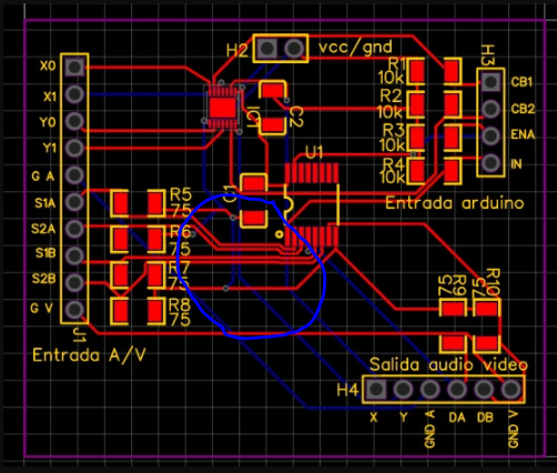
Hello, I am designing a PCB usign in part of it the ts5v330, however i am not sure if i can use it directly with the video signal from RCA STB thru this IC to the output for a TV, i found a PDF mentioning a 75 Ohm resistor in parallel to the input and output, is it correct? should I add this resistor to each input and to the output if i am using a RCA signal from a STB? also do you recomment use a desacopling capacitor between VCC and GND?

  • Hey Eduardo,

    I'm sorry, i'm not quite following. Could you send a block diagram or schematic of rough drawing/figure of what you mean? Sounds like you're attempting to short the input and output with a 75ohm resistor.

    A decoupling cap between Vcc and GND isn't necessary but they're a nice addition to ensure you'll see consistent functionality. So not necessary, but it would only help the system. 

    Thanks,
    Rami Mooti

  • Hello Rami, thank you for your answer, no I dont mean to put in short the input with the output is to put a resistor at the input to GND one resistor for each one, and one for output, I will attach the picture about what i am refering to, my question if this a basic require for this IC or it is optional for better work, my doubt is to decrease too much the video signal at the input and the output with these resistors

  • Eduardo,

    Oh i see. These appear to be for matching the characteristic impedence. Video applications have 75ohm terminations to keep the line the same resistance to ensure there isn't any reflection which results in signal distortion. So you want the same impedance at the load as you do on the source. TS5V330 has a low On-Resistance, R-on, (this varies depending on your supply and signal characteristics) so it should seem fairly 'invisible' to the line. That's to say its effects are minimal. You can even see that we tested the R-on with a 75 load in mind as 75ohms is the coaxial resistance conventionally used.

    So to answer your question directly, this would depend on the source and load impedance, but you would want the impedance from source to load to be the same. But the TS5V330 doesn't handle this characteristic impedance itself. Instead, the aim is to mitigate the effects by keeping the R-on low.

    Hope this helps,
    Rami Mooti

  • Hi Again Rami, thank you for your answer, it was not so clear for me, the video source will be a component video (RCA yellow cable) from a STB, a dvd, etc thru this IC, to the output will be connected to a TV, so i will use this as switch for differente sources to a common  TV, in this case all the inputs will be Component, so the impedance is 75 Ohm for each one and an also for the output, in this case, should I put also a 75 Ohm resistor as the diagram above? what is your recommedation?

  • Eduardo,

    With the addition of the TS5V330 in the line, you should be fine without the 75ohm resistor on the board as the source and load have the same impedance. Here's some information i pulled for guidelines on PCB board layout from another high speed mux, TS5MP646, that can be useful too.  

    • Place the supply de-coupling capacitors as close to the VDD and GND pin as possible. The spacing between the power traces, supply and ground, and the signal I/O lines, clock and data, should be a minimum of three times the race width of the signal I/O lines to maintain signal integrity.
    • The characteristic impedance of the trace(s) must match that of the receiver and transmitter to maintain signal integrity. Route the high-speed traces using a minimum amount of vias and corners. This will reduce the amount of impedance changes.
    • When it becomes necessary to make the traces turn 90°, use two 45° turns or an arc instead of making a single 90° turn.
    • Do not route high-speed traces near crystals, oscillators, external clock signals, switching regulators, mounting holes or magnetic devices.
    • Avoid stubs on the signal lines.
    • All I/O signal traces should be routed over a continuous ground plane with no interruptions. The minimum width from the edge of the trace to any break in the ground plane must be 3 times the trace width. When routing on PCB inner signal layers, the high speed traces should be between two ground planes and maintain characteristic impedance.
    • High speed signal traces must be length matched as much as possible to minimize skew between data and clock lines.


    Rami Mooti

  • Hey Eduardo,

    I haven't heard back in a couple weeks, so i'm going to close out this question. Feel free to respond and reopen it if you need anything else!

    Rami

  • Thank you Rami, well, i bought the ts5v330 to check, i follow the recommendations and create a pcb for test only, anyupdate i will report, thanks

  • Hello Rami, here again, well I got all the components and i did the test circuit, I dont know if I did it wrong:

    1. I found out there is not need for external power to power up the IC, with the same Video power works

    2. Even i tried different options for  in input there is not any switching at the ic, the input video is in every output even if there is should not be

    3. with ena high the IC should be off, however is still on

    4. the capacitors are not so needed, just prevent "a noise" to been seen

    5. The 75 Ohm resistor are HIGHLY needed, without them the images are not clear and/or complete.

    6. please check the desing circuit and tell me if I am doing something wrong here

  • Eduardo,

    A couple of questions here, What is H2? it almost looks like you're driving VCC to GND through the GND pin here? 

    S1A/S2A and S2A/S2B are two video sources and the DA/DB are the video output right? Could you try testing this with just a regular low voltage signal to see the switching characteristics?

    Have you also checked the traces without the device? Or continuity across the pin traces?

    Thanks,
    Rami

  • Hello H2 is just a name for the pin for VCC and GND.

    Yes S1A/S2A are video inputs, and DA are output video, well the Video signal is 500mV and 6.5mA, but you mean with a DC input signal? what voltage do you recommend to test?

    No, I didn't check the traces, i did a 2 IC test board. But the other IC works fines in the same board. below is the desing for the board

    What else can i do for test? what about the diagram, it is ok?

  • Eduardo,

    Any signal that is within the recommendation would be fine. A DC signal with low current (this device can handle +-128mA on the switch) is typically just easier to work with. Something just like a 3.3V signal from say an MCU or power supply you have would be fine. 

    Thanks for sharing the PCB outline, and explaining H2. Okay this makes since. 

    What frequency level are you working with?
    So immediately looking at the board i'm concerned with the spacing between the traces and the thickness of the traces too. Are the lines themselves impedance matched? It looks like all the traces are the same thickness across the board.

    This is from the design recommendations above:

    All I/O signal traces should be routed over a continuous ground plane with no interruptions. The minimum width from the edge of the trace to any break in the ground plane must be 3 times the trace width. When routing on PCB inner signal layers, the high speed traces should be between two ground planes and maintain characteristic impedance

    This area concerns me as it looks like you've run your signal lines side by side for quite some time with little to no isolation between the traces.

    Thanks,
    Rami Mooti

  • Ok Rami I understand that, but if there was not enoght isolation between lines should be a noise on the signal? at the output? well right now the image is fine, the problem is the IC is not doing that it suppose to do, switching, I think the separation lines right now is not a issue for the behavior for the IC, only get some problems, in any case for the quality of the signal right?

    For the other part, why is not doing the right behavior? can you help me with a test circuit to do a switch behavior?

    and for the desing and component location it is ok the connections?

    Can the IC been damaged for high temperature at the moment for welding? was used 350 degrees to weld, I can not find another explanation about what is wrong

    Please your help

  • Eduardo,

    There are some test circuits shown in the datasheet such as figure 6, 7, 8. If you're really just interested in the switching characteristics, you could remove the network analyzer in the circuit with a scope on Dx and place a voltage source on one of the Source pins. Then simply select the path you want by changing the ~En/In according to the logic. 


    The layout looks okay minus what i mentioned previously. You may be better off trying to reorient the chip to allow for more spacing. You also look like you have some 90degree angles on your traces that need to be handled. For example, you have 2 traces being fed into the GND pin of the device that form a 90.
    How is Da handled? Is this a trace on the back of the board?

    Unfortunately yes, this could be a problem. Especially if you're holding it at that temperature. The MSL rating/peak reflow temperature is listed in the product page. Here you see it's 260C.

    I've attached a link, Here, to a good threat with some more information about soldering and reflow temperatures.  If by welding you mean soldering, here's another good source : www.ti.com/.../snoa549d.pdf


    Thanks,
    Rami Mooti

  • Hello, thanks for your answer, indeed i think is a damage for temperature, because was welded at 350 instead 260, because the images is clear and fine, only the IC is not working, I will buy again this IC and try to weld it at 250, i will let you know any update, thank you

  • Eduardo, I think you may be right.
    Good luck with this and I hope it works properly with the new part!

    In the meantime, i'm going to close this thread but don't hesitate to reach out and update me if any new information or problems arise. 

    Thanks,
    Rami Mooti