This thread has been locked.

If you have a related question, please click the "Ask a related question" button in the top right corner. The newly created question will be automatically linked to this question.

TS3A5223: About the behavior when switching

Part Number: TS3A5223
Other Parts Discussed in Thread: TMUX1237,

Currently, this IC is used as follows.
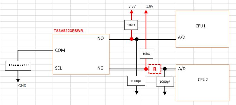
One thermistor is connected to microcomputers with different drive voltages, and they are switched and used depending on the situation.
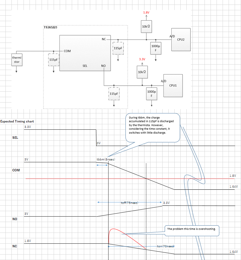
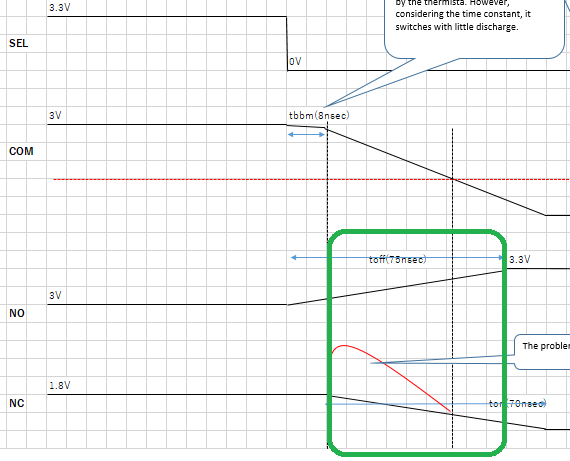
For example, when the thermistor is set to 100kΩ and COM and NO are connected, 3V will be applied to CPU1.
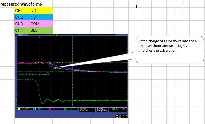
Next, when the COM connection destination was switched to NC, a voltage exceeding 1.8V was transiently applied to CPU2.
If no measures were taken, it would have exceeded about 0.5V at room temperature with n = 1.
When I put 1kΩ in R of the dotted line in the figure below as a trial, it was suppressed to about 0.1V.

In addition, Vcc uses 3.3V input and SEL uses 0 / 3.3V input.

So I ask.

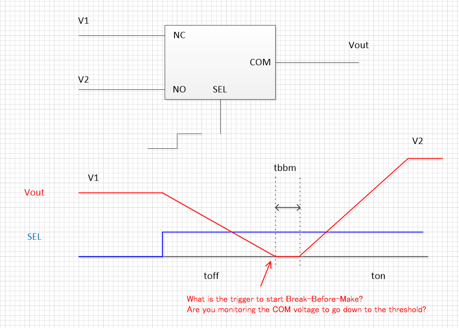
1.  Is this behavior as expected?
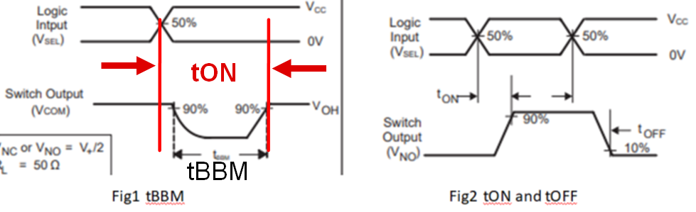
2. It seems that COM, NO, NC are turned on at the same time transiently, but is it possible in principle?
3. If it is as above, is there any other good countermeasure?
4. If we try to add R as shown in the figure below, is it possible to designly suppress how much value should be entered?
In other words, is it possible to indicate how long it will take to turn on at the same time as a design or ability value?

Best Regards.

  • Hello,

    Thank you for your question and welcome to E2E!

    It seems that the image you are referring to is not showing in the post. Could you try re-posting the image, maybe as an attachment?

    Let me see if I understand your question-- is the following statement your main concern? "If no measures were taken, it would have exceeded about 0.5V at room temperature with n = 1."

    Are you observing that the voltages at CPU1 and CPU2 are 0.5V above the expected voltages (3V, 1.8V)?

    Could you help me understand your 2nd question: are you asking about the time taken to switch from NO to NC? Or, are you asking if there is any delay from input to output of a channel, for example COM to NC?

    Best regards,
    Kate

  • Hello, Kate.

    Thank you for your quick response.

    sorry. I'll send you the file again.

    My concern is the cause of this phenomenon and how to deal with it.

    The following is just an explanation of this phenomenon.

    "If no measures were taken, it would have exceeded about 0.5V at room temperature with n = 1."

    The second question I wanted to know was about the time taken to switch from NO to NC.

    Best regards.

  • Hello,

    Thank you very much for the image block diagram, this is very helpful for me to understand your system. 

    I want to double check that I understand before I move forward with helping you troubleshoot. VCC is 3.3V and SEL voltage levels are 0V/3.3V. You are observing nominal voltage at NO, 3.3V, when switch is connecting COM to NO. Where you have a concern is when COM is switched to NC and the transient voltage at NC is higher than 1.8V (by 0.1 to 0.5V, depending on the presence of R). Is this correct?

    Have you measured voltage at the COM node (at thermistor) during all cases? And, thermistor is set to 100kohm during all cases?

    Regarding switching time from NO to NC, I would like to point out a few things from the datasheet. This device has the break-before-make feature, which ensures that NO and NC will never be shorted to COM at the same time. This means that there will always be a minimum switching time from NO/NC-- characterized by tBBM in the datasheet. Typical tBBM for this device is 8 ns. Because there is no enable pin in this device (only SEL, so the switch cannot be set to "high-Z"), the timing specifications tON and tOFF characterize the maximum switching time from NC/NO (70 ns) or NO/NC (75 ns). 

    Best regards,
    Kate

  • Hello, Kate.

    Thank you for your response.

    >I want to double check that I understand before I move forward with helping you troubleshoot. VCC is 3.3V and SEL voltage levels are 0V/3.3V. You are observing nominal voltage at NO, 3.3V, when switch is
    >connecting COM to NO. Where you have a concern is when COM is switched to NC and the transient voltage at NC is higher than 1.8V (by 0.1 to 0.5V, depending on the presence of R). Is this correct?
    Yes. Your perception is correct.

    >Have you measured voltage at the COM node (at thermistor) during all cases? And, thermistor is set to 100kohm during all cases?
    Wrong. The resistance value of the thermistor changes depending on the ambient temperature.100kΩ is an example.
    10 kΩ at 25 ° C. The resistance value drops at high temperatures. The resistance value increases at low temperatures.

    >Regarding switching time from NO to NC, I would like to point out a few things from the datasheet. This device has the break-before-make feature, which ensures that NO and NC will never be shorted to COM at the
    >same time. This means that there will always be a minimum switching time from NO/NC-- characterized by tBBM in the datasheet. Typical tBBM for this device is 8 ns. Because there is no enable pin in this
    >device(only SEL, so the switch cannot be set to "high-Z"), the timing specifications tON and tOFF characterize the maximum switching time from NC/NO (70 ns) or NO/NC (75 ns).
    I understand that it doesn't turn on at the same time. Then, is the cause of this time the input capacity of COM? (115pF)
    In the above case, what is the maximum input capacity of COM according to the design value?
    Is this method correct? (Add resistor)

    Best regards.

  • Hello,

    Thanks for the additional information. I have one more question-- what is the purpose of the two 1000pF capacitors in your system block diagram? Are these intended to be decoupling capacitors for the voltage sources or serving a different purpose?

    Here are my thoughts on the addition of the resistor R: By adding R, you are creating a parallel resistor network (R in parallel with the thermistor + Ron of the switch). The resistor R is decreasing the equivalent resistance of the switch network and potentially undermining the effect of the thermistor in your system and therefore lowering the node to your expected voltage. This leads me to believe that there is an issue elsewhere in the system, likely with the thermistor/system temperature, that is causing the unexpected behavior, this is something you may want to investigate. The Ron flatness of the switch is very small, it is unlikely that the switch is a factor in this behavior, unless absolute maximum ratings are not being observed, such as excessive input/output current. Have you measured the current through your switch/resistor network?

    The on-capacitance specification provided for input/output COM is 115pF, which is a factor in turn-on/off time. I recommend that you watch this TI Precision Labs video to learn more about switch on-capacitance and its effect on switch timing.

    Best regards,
    Kate

  • Hello, Kate.

    Thank you for your response.

    1000pF has two purposes. One is noise suppression. The other is to reduce the impact of the input capacity of the A/D port.

    By the way, is there a capacity limit that can be attached to the outside?

    I think that R is not the cause because there is a problem even if I do not add R.

    I am sorry. Therefore, the current is not measured.

    In addition, the input resistance of A / D is large enough, R does not affect the measurement results.

    I will send you the cause that I am assuming here by attachment now, so please confirm the contents.

    I have an additional question.

    When I look at the data sheet, I can read it as follows, but what about it?

    Best Regards.

  • Hello,

    Thank you for the very detailed information, I understand what you have shared. There is no constraint on how you design external I/O capacitance in this case, but these capacitance values-- especially at COM-- can be adjusted to help mitigate overshoot. I highly recommend reading the following FAQ article about debugging overshoot. Then, look at TMUX1237 as an updated switch for your system that may help you prevent overshoot in your application.

    The Break Before Make delay occurs at every switching event, meaning it is triggered by a change in control signal. This feature ensures that no two signal paths are shorted during switching time. This is characterized in the datasheet as a timing delay with detailed parameter measurement information to give system designers an understanding and expectation of the switching time. How the actual voltage of the signal is affected depends on loading conditions and system parameters.

    Best regards,
    Kate

  • Hello, Kate.

    Thank you for your response.

    Immediately I see TMUX1237 .

    By the way, "The Break Before Make delay occurs at every switching event, meaning it is triggered by a change in control signal. "

    means that it will be turned on at the same time during the green square in the figure below?

    (It doesn't occur with tbbm >> toff.)

    Best regards.

  • Hello,

    I do not see a change in SEL in the range of the green box. tBBM will apply during change in SEL input as in Fig 1 below. BBM states that there will be a minimum time where the signal path is "disconnected" due to change in SEL. Your system varies from the test conditions below, your COM doesn't  discharge enough before connecting to NC, causing overshoot. I recommend adjusting capacitance to allow for a faster discharge, calculating using the switching time measured in your own system (from the scope shot you provided) rather than trying to recreate an illustration from datasheet interpretation.

    tON and tOFF are characterized as the maximum switching time in response to change in SEL, since you are facing an issue with "too little" time for discharge, I would not be concerned with the maximum tON. 

    Please let me know if you have received sufficient help.

    Best regards,
    Kate

  • Hello, Kate.

    Thank you for  the detailed explanation.

    At last, I could understand the internal operation of this IC.

    But the ”a faster discharge” you recommend is not possible for me.

    The reason is that the resistance value of the thermistor changes greatly depending on the operating temperature.

    In addition, in our usage this time, the port may be switched even when the thermistor is not connected.


    As I asked before, is it difficult to provide a design value for the COM input capacity?


    Best regards.

  • Hello,

    The COM input capacitance characteristic is provided in the datasheet as "(CON) NC, NO, and COM input capacitance when switch is on" in the Electrical Characteristics section. This is 115 pF for TS3A5223 and 21 pF for TMUX1237. These values have been characterized with the given load conditions and test set-up provided in the datasheet.

    Best regards,
    Kate

  • Hello, Kate.

    Thank you for your response.


    I know it's 115pF(typ).

    I would like to know the maximum input capacity, please tell me.

    If it's difficult to answer, just tell me the order?  2x, 3x, 5x?

    In addition, is the input capacity of each port for each individual almost equal? Or do they change apart?

    Do both of the following two examples exist?

    example 1 : COM=100pF, NC=105pF, NO=95pF

    example 2 : COM=150pF, NC=85pF, NO=110pF

    Best regards.

  • Hi,

    The maximum input capacitance specification is not provided for this device. Customers may choose to design their systems using the typical specification for each input/output pin. Using this typical specification, under same conditions you may design for similar behavior across I/O pins.

    Best regards,
    Kate

  • Hello, Kate.

    Thank you for your response. And I'm sorry for the late thank you.

    I understand the contents of the answer.

    Doesn't it mean that you don't recommend using anything other than the datasheet conditions?

    Best regards.

  • Hello,

    Electrical Characteristics, such as on-state input capacitance, provided on the datasheet are characterized under a certain set of test conditions. These characteristics give designers an understanding of how the device operates at these conditions. The conditions for your system design may certainly vary based on your design requirements.

    While your system-level design conditions may vary, it is important to stay within the Recommended Operating Conditions of the device. Stresses beyond those listed under "Absolute Maximum Ratings" may cause permanent damage to the device. These are stress ratings only and functional operation of the device at these conditions is not implied.

    Best regards,
    Kate