This thread has been locked.

If you have a related question, please click the "Ask a related question" button in the top right corner. The newly created question will be automatically linked to this question.

TS5A3157: The charge pump leakage of ts5a3157

Part Number: TS5A3157
Other Parts Discussed in Thread: SN74CB3T3257, SN74LVC1G3157, SN74CBT3257

Hi, Team,

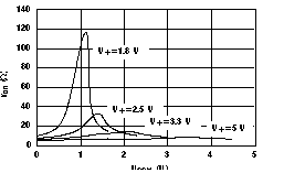
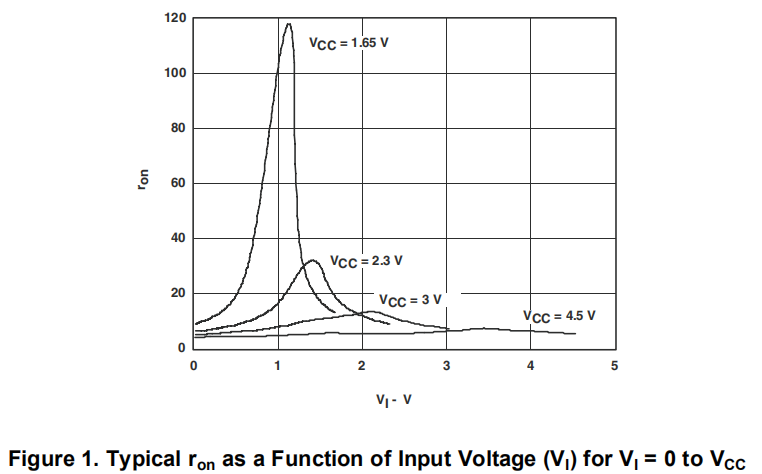
We are considering using ts5a3157 in  a sampling detector circuit and not lack of informantin about the  noise performance. Per our understanding , there must have  a charge pump inside  and if we use the VCC=5V,

does the pump work in that condition?  If does, what would be the leakage to signal path and how is the frequency?

Best Regards,

James

  • This device does not use a charge pump; figures 1..3 show the typical characteristics of a transmission gate. You do not have to care about noise generated by the switch itself.

  • Hi, Clemens,

    Many Thanks!

    Per our understanding, as the device support VCC 1.8-5.0V ,the N-MOS switch gate  need at least 2.5v  voltage  higher than the input signal to keep the switch conduction. So there have using the charge pump. Am I right?

    Best Regards,

    James  

  • Hi, Clemens,

    Further  information in the similiar part SN74CB3T3257 detail the Vgate=VCC+VT , should be a charge bump inside?

    Best Regards,

    James

  • A transmission gate consists of two transistors. As shown in figure 1, near 0 V, the N-MOS conducts very well, near 1.8 V, the P-MOS conducts very well, and near 1.1 V, both transistors are near their threshold voltages and almost off.

  • Hi, Clemens,

    Many Thanks!

    The circuit from datasheet of  TS5A3157 show that it just have one N-MOS switch in each dirrection. Please refer to the attached. The similar one ,sn74lvc1g3157 do have two in each dirrection. Comparing the curve your attached with the one from sn74lvc1g3157, their are nearlly the same,  which confuse me that if there have bump inside. 

    Would like to have your further advice.

    Best Regards,

    James  

  • Hi, Clemens,

    Further information, in figure 3 from datasheet of  TS5A3157 , the Max VCOM could be equal to the VCC 4.5V and the N-MOS still can conduct with only 6 Ohm resistance, which also confuse me.

    As our sampling detector will handle the weak signal as low as 2-3uv, we are more concern about the noise figure of the device itself.

    Would like to have your further advice.

    Many Thanks & Best Regards,

    James  

  • The block diagram is just wrong.

    The resistance is lower at higher supply voltages. You see the same curve for 5 V in figure 1.

  • Hi James,

    Clemens in correct - the block diagram in the datasheet does seem incorrect as the on resistance plot that Clemens has shared is for the transmission gate architecture.  This device can pass rail to rail due to  it using NMOS and PMOS FETs. It doesn't have a charge pump. When you say noise addition from our device could you please elaborate on what you are looking for exactly - as we don't add noise FOM's typically to mux datasheets. However we do spec charge injection and leakage which will have an effect on system accuracy. 

    Please let me know so I can see if we have the correct information you are looking for. 

  • Hi, Clemens,

    Many Thanks! You help much!

    Hi, Parker,

    If the  TS5A3157 have the same switch circuit as the  sn74lvc1g3157 ,what would be the main advantage  comparing to the later one? 

    This part is going to use in a sampling detector and as it will handle the weak signal as low as 2-3uv, we are more concern about the noise introduced by the device itself. If there have not any oscillator inside, it will fit the requirement . 

    The second requirement is the switching speed. The detector is switching on 70Mhz and It seem that the  sn74lvc1g3157  will faster than the TS5A3157 , right?

    If the sn74cbt3257 ,which just have NMOS switch, will be the more suitable one? 

    Best Regards,

    James

  • Hi James,

    With a detector speed of 70MHz either the TS5A3157 or the SN74LVC1G3157 will be able to handle that frequency without much attenuation. While the LVC device does have a higher bandwidth both parts will support the signal. However the TS5A3157 has a lower leakage current - this does add error to the switch we have a typical on leakage of 5 times lower with the TS5A157 than the SN74LVC1G3157. So I think both devices would work here but I'd suggest the TS5A.

    I wouldn't use the sn74CBT3257 as it seems to be a NMOS switch which will inherently down-translate. Also the way we used to measure Ron doesn't give the full idea of Ron changes versus input voltage. I would suggest teh TS5A3157 out of the devices you are looking into as it shouldn't add noise due to there being no oscillator.

    If you have any other questions please let me know!

    Best,

    Parker Dodson  

  • Hi, Parker,

    Thanks for all!

    Got your ideal.

    Best Regards,

    James

  • Hi James,

    No Problem! 

    If you need anything else just let me know!

    Best,

    Parker Dodson