This thread has been locked.

If you have a related question, please click the "Ask a related question" button in the top right corner. The newly created question will be automatically linked to this question.

TMUX1308-Q1: Injection Current Coupling

Part Number: TMUX1308-Q1
Other Parts Discussed in Thread: TMUX1308

Hi, Team,

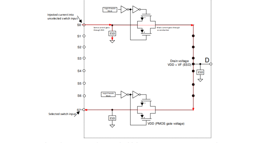
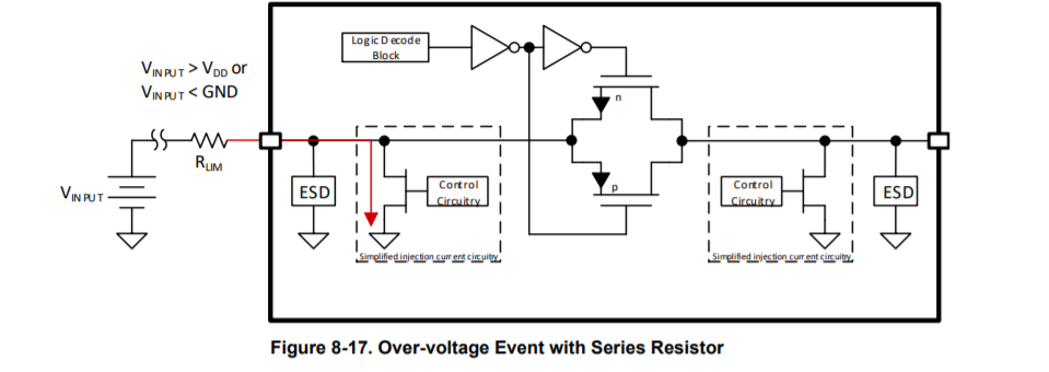
This part has Injection current protection internally at both Sx and D pins.

It has been described that Injection control circuitry becomes active when input(Sx) is disabled by the logic pins and the injected current causes the voltage

at the pin to be above VDD or below GND. 

What voltage does the D terminal output have when an injection current flows into the enabled signal input?

Best regards,

H.Someno

  • Hi Hidekazu,

    In Figure 7-13 of the datasheet it shows the maximum shift in output voltage for the amount of current injected. The output doesn't care what the source of the injected current is - it only cares that there was current Injected. Please see figure below to see shift in output voltage due to injected currents:

    If you have any other questions please let me know!

    Best,

    Parker Dodson

  • Thanks for your reply.

     I have additional inquiries to your comments and TMUX1308-Q1 functions.  Would you please tell me about them?

    1. About your reply:  Are you meaning that OUTPUT(one D pin for TMUX1308) voltage is determined by the operation of the progression circuit at the D terminal, regardless of which input terminal the current is injected into?
    2. When the current is injected into an enabled input(S), how does the injection current protection circuits built in both that injected input pin and output pin take an action?
    3. Section 7-9 on datasheet shows the specification table for delta-VOUT with Rs resister against Iinj current. I understand the test circuit is based on Figure 8-11(the conditions where the injected current is applied to a disabled input ).                                                                                                                     What kind of measurement circuit was used to measure the graph data in Figure 7-13?  Is there any relationship with specifications table in section 7-9?

     Regards,

    H.Someno

  • Hi Hidekazu,

    1. The voltage output Vd during a current injection event is as follows:

    a) A Channel is selected lets say S0, so the enabled signal path is S0 to D. Under normal conditions the input Voltage Vso is approximately Vd.

    b) However if a current is injected into an off channel (This scenario S1 - S7) the output voltage Vd = Vso + V_current_injection_error.

    c) The error due to injected current is found in the figure I provided

    Since the input is known as the voltage source, the error will show itself at the output when current is injected into a disabled channel. To see this pathway a bit more clearly please see below:

    Due to the injected current pathway error on the output is what is being measured.

    2. For an overvoltage event the excess current is going to be routed through control circuitry. In this mode the current control acts as a clamp to absorb excess current while limiting the impact of the injected current. The Injected current will still have an error associated with it that is going to be similar to the first plot I shared in my first response.

    To avoid damage though we still recommend current limiting resistors to keep the single channel injected current <= |50mA | while keeping the total injected current at any one time to the device <= |100mA|

    Below shows the eq. circuit of injected current events for selected pins.

    3. Both the table in 7-9 and Figure 7-13 use the same test circuit - 8-11- but they are showing slightly different things. 

    The Table in 7-9 is giving typical values as well as max values for specific conditions of how much current is injected and the source impedance. It only hits current injections <= 10mA.

    The Figure in 7-13 shows a typical response curve of Voltage shift vs. Injected current - this extends to 50mA unlike the table in 7-9. Based on the curves that are being shown - this is the low Rs value case as the smaller the source impedance is the less error is shown. I apologize that can be a bit confusing from looking at the datasheet.  

    If you have any other questions or any needed clarifications please let me know and I will see what I can do!

    Best,

    Parker Dodson

  • Parker-san,

    Thanks for the detailed explanation.

    I'm sorry to be persistent. From the contents so far, I now understand as follows. Is these understandings all right?

    - The injection current protection circuitry works even if the current injection( or over voltage like >VDD or <GND) happened to the source of enabled path(Figure 8-17 of datasheet is explaining it.)

    - The Delta VOUT spec  specified in SECTION 7-9 of datasheet is adapted not only when an injection current occurs at the source(S) of the disabled path, but also when an injection current(or overvoltage) occurs at the source pin(S) of the enable path.  And In case of larger injection current, Figure 7-13 of datasheet shows it.

    Regards,

    H.Someno


  • Hi Hidekazu,

    No need to apologize, I am here to help! 

    -Yes the current injection control circuitry operates when current is injected into a disabled channel or when the input voltage is > VDD or  < GND leading to a current injection event on a selected pin.

    - With Table 7-9, it shows what you can expect for a ranges of source resistances and currents injected. This is for currents injected <= 10mA.  It is specifically tested on a disabled channel - however the results of the table can be extrapolated to the overvoltage case as a good guideline as the error should be similar as the error is due to the current injection. 

    - Figure 7-13 shows a typical curve for current injected into a disabled channel. You are correct it is over a larger range of injection currents.  It is a good approximation of what you can expected for a current injection event with a lower source resistance. 

    For designing with the device - using the data in 7-9 and 7-13 are good guidelines to follow for output voltage shift due to current injection events - regardless if the current injection events are from a disabled channel or a over/under voltage event on a selected channel. Be sure to make sure less than 50mA ever go into one port as an injected current - and the device can only handle 100mA between all channels at any one time.

    If you have any other questions please don't hesitate to reach out!

    Best,

    Parker Dodson

  • Parker-san,
    Thanks for your detailed comments.

    Now I received additional questions about the operations at the specific measurements.
    So, I would like to switch to local communication. Since I send you new inquiries from customer later by email, so please support them.

    Best Regards,

    H.Someno