This thread has been locked.

If you have a related question, please click the "Ask a related question" button in the top right corner. The newly created question will be automatically linked to this question.

TS5A3166: Impedance between NO and COM

Part Number: TS5A3166
Other Parts Discussed in Thread: TS3A24159

Dear team, 

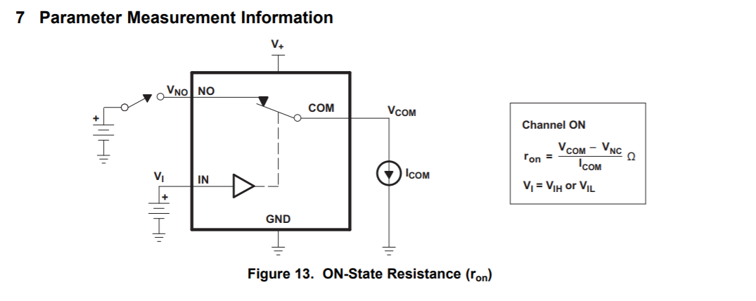
My customer consider using TS5A3166 for Current Transformer application.but there is issue on that. 

- Vcc : 3.3V

- IN signal : high , Rds on 0.9~1.1 ohm It is OK. but IN signal : Low, resistance between NO an COM is measured 10K ohm ~60Kohm. Is it possible? 

If Vcc is off, resistance is over several M ohm. please let me know your opinion. 

Thank you. 

  • Dino, 

    This doesn't seem right. The max "Off resistance" should be a lot higher. To calculate this you can use the Off leakage current characteristics in the datasheet. You'll find the I and R needed for your V/I = R equation. Here's a post about this I found with an example:
    https://e2e.ti.com/support/switches-multiplexers/f/388/t/919731?tisearch=e2e-quicksearch&keymatch=the%20%E2%80%8Eresistance%20value%20in%20case%20of%20switch%20OFF

    Depending on your test conditions, you should be seeing a resistance a few factors above this. Closer to 15Mohms.

    It seems it may be damaged. Do you have another chip you can check this on?

    Thanks,
    Rami


  • Hello Rami, 

    Thank you for your response. 

    I think also that above M ohm resistance is right as off status resistance, so the customer checked another sample (5 ea) but the result same, 10K~60K ohm resistance between NO and COM port. 

    Is there any scenario where we can see these results like abnormal test setup or GND connection? The customer also tested TS3A24159 but similar results. 

    Please review again and let me know your opinion. 

    Thank you. 

  • Dino,

    How are they measuring R-on? Are they running the test as shown in the datasheet?

    Thanks,
    Rami

  • Dear Rami, 

    They didn't measure as shown in the datasheet. They measured Ron/ Roff just using multi-meter between NO and COM. 

    Can this be a reason of abnormal resistance? please let me know. 

    I found abnormal voltage at IN port during test. When V+ injected, why we can see 0.7V ~2.7V voltage on IN port? 

    Thank you. 

  • Dino,

    This could be the reasoning for the abnormal resistance. The Ron values are dependent on the Vgs voltage, not just the voltage at the input. Using a multimeter doesn't give any current control so it's easy to saturate the current, so more current than needed would be used and the resistor value would be lower than it actually is (Think R = V/I. As I increases the R goes down) You could even overheat the device without current control. Which is why we recommend using a current source. 
    Depending on the multimeter you could accidentally input more current than the chip can handle when probing. 

    With regards to the abnormality you're seeing, there could be many problems here. Is this problem only present on one chip or is this a consistent problem on all chips? Could you try to switch the chip out.
    Furthermore, you could try shorting out the input and output with a resistor and see if the problem is still there?
    And just as a sanity check, I would make sure that there aren't any shorts on the traces on the board itself. A simply continuity check should from Vcc to IN would be good to do.

    Rami  

  • Hello Rami, 

    Thank you for your comment. 

    This problem is present on all chips(5 ea). I am sorry to bother you but please review below questions and let me know your opinion.

    1. The customer want to use SPST(TS5A3166) to add parallel resistor at Current transformer output to MCU input line. If this issue is by multi meter current, Can we use SPST(TS5A3166) for this application?     

    2. You could try shorting out the input and output with a resistor =>  Which port do you mean input and output? and 0 ohm resister?

    3. How about Oscilloscope test? Oscilloscope is same situation with multi meter. please review below waveform. Is this waveform normal? 

    1).Waveform #1 : ON status - V+ : 3.3V , IN : 3.3V(High), NO : 3.3V(Green) ==> COM : 3.3V(Blue) 

    - I think turn on status is normal 

    2). Waveform #2 : Off status - V+ : 3.3V , IN : GND(Low), NO : 3.3V(Green) ==> COM : Blue 

    - I think turn off status is abnormal  

    3).Waveform #3 : floating status : - V+ : 3.3V , IN : floating, NO : 3.3V(Green) , COM : Blue 

    Thank you. 

  • Dino,

    This is not proper behavior of the chip.
    Whether this part would work depends on the signals being used. But as long as it stays within the voltage and current levels that the switch can handle, it's fine. Do you have this info? this chip can handle voltages on the supply from 1.65 to 5.5V. At your 3.3V Vcc the Vi/o range would be from 0-3.3V. So you should be fine on that end. The switch can handle up to 200mA. 

    Could you send a schematic and/or block diagram of your setup? If you're seeing 0.7-2.7V at the IN you're switching between ON and OFF and somewhere floating in between. Which is what it looks like you're seeing in the second picture (The OFF status).
    Is the last image the only scope pic showing the IN level?
    The oscilloscope is fine for viewing the voltage/logic levels.

    Rami Mooti

  • Rami, 

    To clarify, There is no MCU and signal source connected NO and COM port. just device test on test board.

    <Test set up> 

    1. Waveform #1 : turn on status

    - V+ : 3.3V  power supply / - IN port : tied up V+

    - NO port(Green) : tied up V+(3.3V  power supply)  ==> COM port(Blue) : 3.3V output , OK

    2. Waveform #2 : turn off status 

    - V+ : 3.3V  power supply / - IN port : tied up GND

    - NO port(Green) : tied up V+(3.3V  power supply)  ==> COM port(Blue) : abnormal output

    => You mentioned there is floating status but only IN port tied up GND but we can see like triangle waveform. I don't understand this waveform. please let me know your opinion regarding this waveform. 

    3. Waveform #3 : floating status  (Red waveform is IN port) 

    - V+ : 3.3V  power supply / - IN port(Red) : floating 

    - NO port(Green) : tied up V+(3.3V  power supply)  ==> COM port(Blue) : abnormal output

    => I don't understand why we can see same like triangle waveform on COM port under IN port is GND or floating level. please let me know your opinion. 

    <Request>  

    1. please review test setup and waveform #1~3. and let me know your opinion. I tried several device but I got a same results. 

    Thank you. 

  • The set up seems fine. 

    Could you probe the IN with both conditions 1 and 2. Mainly i'm interested in #2 where we think IN is grounded but i want to confirm that it's actually grounded.
    With V(IL) being 0.8V and V(IH) 2.0V, my feeling is that when it's floating the switch is just turning on and off as it enters that inbetween voltage zone where we can't confirm the level. Which is okay when floating because that isn't the recommended operational use case. 
    However, when IN should be grounded it looks like it still may be floating, which shouldn't happen. Have you checked continuity of the ground input to the trace to the pin on the 3166? I want to confirm it's actually grounded by probing the IN signal at the same time. Also just a check of waveform #2 again but adding the IN signal on the scope would be good to confirm as well. Could you check this?

    Just looking to see if the issue is from the test board or some outside source or if we can narrow it down to the chip itself.

    Thanks,
    Rami Mooti 

  • Hello Rami, 

    Thank you for your comment. 

    As you mentioned before, I found there was a issue with the test board and the oscilloscope's probe. so the customer decided making a real board using 3166. 

    I will test again with real board. And then I will contact again you with test result. 

    Thank you.