This thread has been locked.

If you have a related question, please click the "Ask a related question" button in the top right corner. The newly created question will be automatically linked to this question.

CD4051B: Input and output voltage deviation problem

Part Number: CD4051B
Other Parts Discussed in Thread: CD74HC4051, TMUX1308

Hi Team,

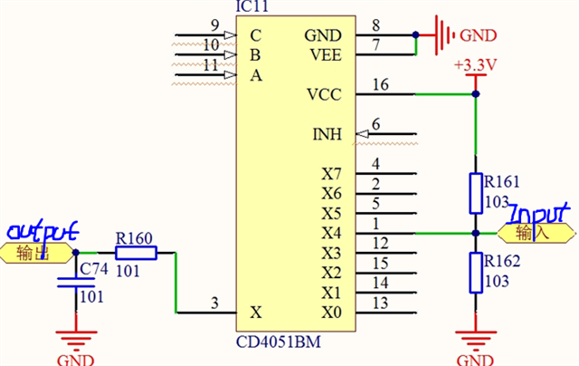
My customer meet some problem in using CD4051, the schematic diagram as below:

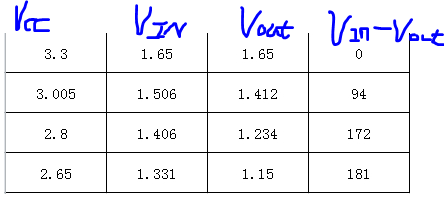
and they find Input and output voltage deviation problem,data show below:

output link to MCU(Large input impedance)and  I think high Ron is doesn't matter, so I would like to know what cause voltage deviation.

(I know that lower than 3v may cause abnormality, but I want to know what is the reason? And there will be a small voltage drop in the 3V power supply, the output signal enters the ADC of the MCU, the customer does not want to see the voltage drop)

thanks for your help in advance.

BR

Jenson

  • CD4000 devices are designed for voltages higher than 5 V. While they will work at 3.3 V, there are no guaranteed electrical characteristics at this voltage.

    At 3.3 V and lower voltages, the transistors will not be fully switched on, and the on-resistance of the switch will become very high.

    Use the CD74HC4051 or TMUX1308 instead.

  • Hi team,

    thank you for your kindly help.

    I have one more question, why transistor not fully switched on,and the on resistance of switch become high will case the voltage drop?

    According to my understanding, the input impedance of the MCU is very large, so the current is very small. Why does it cause a large voltage drop?

    BR

    jenson

  • CD4000 devices use transistors that can handle high voltages (20 V). Those also have higher gate threshold voltages.

  • Hi Jenson,

    Clemens is correct, once you start getting lower than 3.3V, the channel's pass transistors becomes less conductive, leading to much higher resistances which will be large enough to cause some voltage drop. Why is the VCC changing so much in their design (or maybe this was more experimental)? This part is not designed to support VCC's under 3V.

    Thanks!

    Bryan

  • Hi Bryan,clements

    Thanks for your help!

    yes,this was more experimental .Is the inside of the chip equivalent to a voltage divider network, Vout=(mcu impedance)/(MCU impedance+Ron), the increase of Ron causes VOUT to decrease, is my understanding correct?

    BR

    jenson

  • Hi Jenson,

    You're welcome! That is the correct understanding. You can treat the switch when it is closed as a series resistance with the MCU that will cause a voltage drop to occur due to the increased RON at the lower VCC voltages.

    Thanks!

    Bryan

  • Hi Bryan,

    My customer still have some concern. He believes that the data sheet shows that it can be used at 3V, and the data sheet also shows that the on-resistance is not that large. He believes that the use of 3V should leave a certain margin and no voltage drop.

    So I know, does the power supply below 3.3V actually cause the transistor to produce a large on-resistance (kohm level)?

    Is there no margin for this design(3V will also produce a certain voltage drop)?

    thans for your help!

    jenson

  • For a 5 V supply, the datasheet guarantees that the on-resistance is no more than 1.3 kΩ.
    For a 3 V supply, the datasheet does not guarantee any upper limit.

    As shown in figure 3, the behavior at 5 V already is marginal, i.e., 5 V is already near the threshold voltage. The 3 V resistance will be much larger. And the farther you go below 3 V, the more you are relying on subthreshold leakage (and it is no longer guaranteed that you even get the correct channel).

  • Hi clements,

    Thank you for your help!

    What I think is that the ADC input impedance of the MCU should be very high (maybe to Mohm level), will it produce a high on-resistance at 3V, which will cause the voltage to drop?

    BR

    jenson

  • Typical ADC input impedances are much lower.

  • Hi Jenson,

    Can you provide the part number of the ADC your customer is using? Would help us do further analysis on this signal chain.

    Thanks!

    Bryan

  • Hi Bryan and Clements,

    Thanks for your help.

    As shown in my picture above, the output is connected to  the ADC input port of the MCU (Renesas R5F56519BDFB).he found this phenomenon when testing the waveform with an oscilloscope.Same result when ADC is sampling or not sampling.And the customer believes that from the data sheet, the input impedance is 3M, and the on-resistance will not affect the results.Do you have any suggestions for this

    BR

    jenson

  • The R5F56519BDFB datasheet specifies A/D characteristics for a source impedance of 1 kΩ. For higher impedances, the analog input capacitance will take longer to (dis)charge.

    And for very high source impedances, the input leakage current will result in a voltage drop.

    The CD74HC4051 is pin compatible and actually works at those voltages.

  • Hi Clemens,

    I understand higher impedances will take longer time to charger or discharger.

    I think on-resistance equal source impedances,but I don't understand why high source impedances will result in voltage drop? what cause leakage current?

    Can you kindly explain to me? thank you for you continue help.

    BR

    Jenson

  • Hi Jenson,

    There will be a current that flows through the switch/source resistance path to the input of the ADC which will cause a voltage drop. Can you provide where in the ADC datasheet they are indicating a 3M ohm input resistance? I do not see anything specified.

    Thanks,

    Bryan

  • Hi Bryan,

    High-impedance reference input current, 3V/0.000001 = 3KK

    For ADC ,I understand higher impedances will take longer time to charger or discharger.But I don’t quite understand how it causes the voltage drop. Can you kindly explain it to me?

    Thanks 

    jenson

  • Hi Jenson,

    Thanks for providing this information. Can you also clarify what the A,B,C, and INH inputs are being set to? The VIH/VIL levels also change as you change the VCC voltage, so if they are not tied to VCC this could pose an issue where the the channel is not being properly selected.

    Thanks!

    Bryan

  • Hi Bryan,

    I have ask my customer, A,B,C and INH follow the VCC voltage.When VCC voltage set low, A,B,C,INH set low too.

    So,It seem not caused by this A,B,C,INH voltage. If you have any other comments?

    Thanks for your help!

    Jenson

  • Hi Jenson,

    It seems like the setup is OK from the digital input perspective then. However, again, when operating at that 3V level, we do not guarantee or know exactly how high that RON will go and you have to be sure that your VCC/digitals inputs are at least 3V otherwise the switch channel will most likely not be fully turned on and the RON will be significant enough to cause a voltage drop even if the input resistance to the ADC is 3M.

    Regards,

    Bryan

  • Hi Bryan,

    Understood,Thank you for your continuous and kindly help!

    BR

    Jenson