This thread has been locked.

If you have a related question, please click the "Ask a related question" button in the top right corner. The newly created question will be automatically linked to this question.

TS3DV642 - Failed HDMI compliance test ID 8-9, line 29, (DDC_SCL voltage)

Guru 19775 points
Other Parts Discussed in Thread: TS3DV642, TS3USB3000

Hi Team,

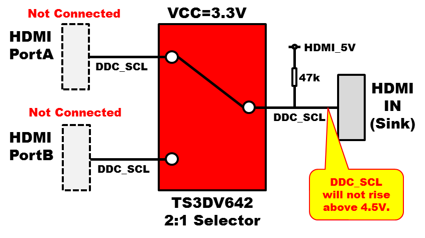
Our customer is using TS3DV642 as a 2:1 HDMI switch. Please see the set up below.
When they practiced HDMI compliance testing, DDC_SCL voltage were not able to keep over 4.5V when both HDMI port is OPEN.
If VCC of the device is increased up to 4.0V, DDC_SCL voltage met the HDMI spec.

[Q1]
Is there any restriction using TS3DV642 as 2:1 HDMI Input MUX to pass HDMI compliance testing ?

[Q2]
TS3DV642 recommended operating supply voltage is 2.6V to 4.5V. Does customer has any mistake using in below set up ?

[Q3]
Is there any relation between DDC_SCL output amplitude and VCC supply voltage ?

Best Regards,

Kawai

  • Kawai,

    [Q1]

    Is there any restriction using TS3DV642 as 2:1 HDMI Input MUX to pass HDMI compliance testing ?

    No, we have had customers pass HDMI 1.4 and HDMI 2.0 testing with TS3DV642 devices in their systems

    [Q2]

    TS3DV642 recommended operating supply voltage is 2.6V to 4.5V. Does customer has any mistake using in below set up ?

    The set up is within the recommended operating conditions.  Vcc= 3.3 V is within the 2.6 V to 4.5 V range.  SCL = 5V is with in the 0 to 5.5 V range.


    [Q3]

    Is there any relation between DDC_SCL output amplitude and VCC supply voltage ?

    The device uses an internal charge pump to bias the signal path FET so there is no relation between the voltages the SCL pin can pass and Vcc  pin in the TS3DV642 device.  

    The TS3DV642 is a passive FET switch designed to be as close to a 0 ohm wire as possible.  This would lead us to believe that your DDC_SCL bus is being loaded by something else in the system.  

    A) Have you tried removing the TS3DV642 device from the system and seeing if the same issue is present?  

    B) It is strange that you are able to pass with a higher voltage on Vcc.  What else in the system is using the Vcc node for a power source?

    Thank you,

    Adam  

  • Hello Adam-san,

    I had feedback from customer.

    A) They have another HDMI connector design in their system which does not use TS3DV642. This design passes HDMI compliance test. Design is totally the same except for TS3DV642.

    B) They had confirmed VCC waveform and it is meeting the TS3DV642 VCC spec.

    Do you have any advice ?

    Best Regards,
    Kawai
  • Kawai,

    What is connected to the sink? Is there anything else connected to these nodes in the system?

    Can you take scope shots of the input and output of the TS3DV642 DDC_SCL, and the HDMI 5V? So we can see what is happening.

    Thank you,
    Adam
  • Hello Adam-san,

    Thank you for your support and my apologies for my delay.

    For DDC_SCL pins, below is our customer connection.

    SCL : HDMI RX device, 47kohm pull up to HDMI connector 5V
    SCL_A : HDMI connector through 0 ohm
    SCL_B : CPU DDC_SCL

    We are asking for the waveform data.

    Best Regards,
    Kawai
  • Hello Adam-san,

    Could you please allow me to discuss offline ?

    I will send you customer test condition and waveform information material.


    Best Regards,
    Kawai

  • Kawai,

    Thank you for your willingness to share your customer information to find the cause of the problem.  

    We have found that if you are testing an HDMI sink at Test ID 8-9 DDC/CEC Line Capacitance and Voltage there can be a case where the TS3DV642 will cause this line item to fail line 29)

    Line 29 in this test is verifying that the logic high signal is between 4.5 and 5.5 volts. 

    The TS3DV642 has protection diodes from the I/O signal path to Vcc.  If there is signal on the I/O path greater than a diode drop ~0.7 V to Vcc the protection diode will begin to conduct and leak current through supply pin which will cause the voltage to sag on the on the SCL line.  

    There are two ways to help keep the voltages in the passing range during this test.  1) you can raise the supply voltage to the TS3DV642 to keep the protection diode from conducting or 2) use a stronger pull up to 5V rail.  In an HDMI system, a strong pull up of 1.5k ohm is used on the source side so we have only seen this issue show up for sink devices using the weak 47k ohm pull up resistor.   

    Thank you,

    Adam  


  • Hello Adam-san,

    Thank you very much for your support and cooperation.

    As for the SINK application is required to test with no source connection, the only counter measure is to apply higher supply voltage.
    One thing I need to confirm is that recommended operating supply voltage of TS3DV642 is from 2.6 to 4.5V.
    Assuming the device variation, could the device support HDMI Test Spec within this recommended supply voltage range ?

    Best Regards,
    Kawai
  • Kawai,

    The TS3DV642 is a high performance passive FET switch used for many different applications beyond only HDMI switches. The 2.6V to 4.5V recommend voltage range will grantee the specs stated in the electrical specification table including device variation.

    For the reasons mentioned above, if you are running into issues with the HDMI compliance Test ID 8-9 DDC/CEC Line Capacitance and Voltage line item you can solve the issue by increasing the TS3DV642 supply voltage or use a stronger pull up resistor in your application.

    Thank you,
    Adam
  • Hello Adam-san,

    I believe user must take this problem into account when TS3DV642 is used to SINK application and placed right next to the HDMI connector.

    There would be no problem used in SOURCE application or SINK application if TS3DV642 is not placed next to the HDMI connector.

    I also want to inform you that probably both countermeasure would not be acceptable for HDMI compliance testing. Because, schematic cannot be changed just for the compliance test. System design must be exactly the same with the mass production design. 

    > you can solve the issue by increasing the TS3DV642 supply voltage
    TS3DV642 recommended operating supply voltage range is described "2.6V <= VCC <= 4.5V" in the datasheet.
    Drop voltage from VCC may differ by device variation or board design. In some case user may require supply voltage higher than 4.5V.

    > use a stronger pull up resistor in your application
    In SINK application, pull up resistor is designated as 47k ohm and cannot be changed to a stronger value.

    What do you think to my opinion ?

    Best Regards,

    Kawai

  • Kawai,

    Thank you for your comments.  This is the type of engineering community problem solving and collaboration I hope to see continue on the e2e forums. 

    Adam  

  • Hello Adam-san,

    I would like to make sure one thing that if VCC supply voltage is 4.5V (which is recommended maximum), would DDC_SCL pin voltage never drop below 4.5V ?

    Could you please confirm from internal design ?

    I am not sure at what voltage the internal protection diode turns on and how much the leak current would be.
    What would be the estimation from the device design ?

    Best Regards,
    Kawai
  • Kawai-san,

    We are also investigating extending the Vcc range in the datasheet up to 5V to help with issue. Or preliminary analysis is our device will support this voltage but are waiting on enough business to do the full investigation and make the datasheet change. 

    I connected the TS3DV642 signal path to 5V through a 47k ohm pull up resistor.  I varied the supply voltage and measured the voltage at the signal path and how much current is leaking through the signal path.  It looks like as long as Vcc > 3.8 V the signal path will be >4.5 V.

    Does this help?  Let me know if you need any more information. 

    Adam

  • Hello Adam-san,

    Thank you for testing with the EVM. This is a good information and matches with our customer result.

    However, is it possible to provide us a simulation result or estimation based on internal design ?
    We need to convince customer that applying 4.5V could always pass CTS despite of device variation.

    Best Regards,
    Kawai
  • The estimation of the leakage current given by design is (Vi/o-Vcc)/12000 = leakage current.  This is a similar leakage phenomenon as with the TS3USB3000 device and you can see this equation in the TS3USB3000 datasheet.  

    Thank you,

    Adam