Tool/software: Code Composer Studio
Hi, I am trying to define a specific memory location for a variable in the PGA970EVM. However, I am not seeing the variable when I run the debugger. I will really appreciate your help with this issue. Below is the piece of code that should assign the memory location to the variable x. Inside the main, there is code that it is just updating the value as the code is running.
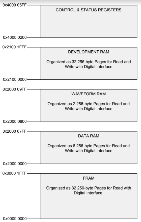
#pragma location = 0x2000000
char x = 0;

void main(void){
 // Code Updating the variable
}