


Part Number: CCSTUDIO-KEYSTONE
Tool/software: Code Composer Studio
Hi,
I am working with 66AK2G12 device. I am trying to check Main PLL configuration by reading follwoing registers:
1. BOOTCFG_MAIN_PLL_CTL0 (addr - 0x02620350)
2. PLLM (addr - 0x02130110)
3. SECCTL (addr - 0x02130108)
I use the default target configuration with evmk2g.gel gel file. The gel file sets up Main PLL.
On connecting to C66 target, gel file output on console is:
C66xx: GEL Output: Starting K2G GP EVM Initialization ..
C66xx: GEL Output: Reading Device Speed from BOOTCFG_EFUSE_BOOTROM
C66xx: GEL Output: DEVICE SPEED[23:16] ---> 1000 MHz
C66xx: GEL Output: ARM SPEED[9:0] ---> 1000 MHz
C66xx: GEL Output: PLL has been configured (24.0 MHz * 250 / 3 / 2 = 1000.0 MHz)
C66xx: GEL Output: ARM PLL has been configured with ref clock 24MHz, -sysclkp_period 41.6666 (24.0 MHz * 250 / 3 / 2 = 1000.0 MHz)
C66xx: GEL Output: Power on all PSC modules and DSP domains...
C66xx: GEL Output: Power on PCIE PSC modules and DSP domains... Done.
C66xx: GEL Output: UART PLL has been configured (24.0 MHz * 128 / 1 / 8 = 384.0 MHz)
C66xx: GEL Output: NSS PLL has been configured (24.0 MHz * 250 / 3 / 2 = 1000.0 MHz)
C66xx: GEL Output: ICSS PLL has been configured (24.0 MHz * 250 / 3 / 10 = 200.0 MHz)
C66xx: GEL Output: DSS PLL has been configured (24.0 MHz * 198 / 12 / 16 = 24.75 MHz)
C66xx: GEL Output: XMC setup complete.
C66xx: GEL Output: DDR3 PLL Setup ...
C66xx: GEL Output: DDR3 PLL Setup complete, DDR3A clock now running at 533MHz.
C66xx: GEL Output: DDR3A initialization complete
C66xx: GEL Output: K2G GP EVM Initialization Complete.
I am expecting following values in registers:
1. PLLM = 0000011111001 = 249
2. PLLD = 000010 = 2
3. CLKOD = 0001 = 1
However, I see these values in Debug -> Register View:
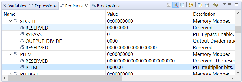
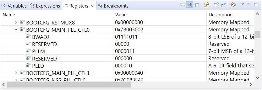
Looks like CCS is able to read BOOTCFG_MAIN_PLL_CTL0 but not PLLM or SECCTL.
I even tried reading them through Expressions, same result:

I then tried using Gel Script function : CORE_PLL_READ_REGISTER_VALUES, and got following output:
C66xx: GEL Output: The value of MAIN_PLL_CTL0_ADDR is 0x7B003002
C66xx: GEL Output: The value of MAIN_PLL_CTL1_ADDR is 0x00000040
C66xx: GEL Output: The value of PLLCTL_ADDR is 0x00000041
C66xx: GEL Output: The value of SECCTL_ADDR is 0x00090000
C66xx: GEL Output: The value of PLLM_ADDR is 0x00000039
C66xx: GEL Output: The value of PLLDIV1_ADDR is 0x00008000
C66xx: GEL Output: The value of PLLDIV2_ADDR is 0x00008000
C66xx: GEL Output: The value of PLLDIV3_ADDR is 0x00008002
C66xx: GEL Output: The value of PLLCMD_ADDR is 0x00000001
C66xx: GEL Output: The value of PLLSTAT_ADDR is 0x00000006
C66xx: GEL Output: The value of PLLDIV4_ADDR is 0x00008004
C66xx: GEL Output: The value of PLLDIV5_ADDR is 0x00008017
C66xx: GEL Output: The value of PLLDIV6_ADDR is 0x00000000
C66xx: GEL Output: The value of PLLDIV7_ADDR is 0x00000000
C66xx: GEL Output: The value of PLLDIV8_ADDR is 0x00000000
I have based an LED toggle on sysclock and am able to achieve correct toggle period using 1GHz as system clock.
Which makes me think that the PLL is actually setup correctly, but CCS is not able to read it.
Can you please confirm if my understanding is correct?
Also can you please explain this discrepancy?
I looked at device xml file and PLL.xml file and couldn't find anything wrong with them.
I am attaching them for your reference.66AK2G12.xml
<module name="PLL" acronym="" XML_version="1.0" HW_revision="n/a" description="">
  <register id="RSTYPE" acronym="RSTYPE" offset="0xE4" width="32" description="">
    <bitfield id="RESERVED" width="3" begin="31" end="29" resetval="0x0" description="Reserved. Read only. Always reads as 0. Writes have no effect." range="" rwaccess="R"/>
    <bitfield id="EMU_RST" width="1" begin="28" end="28" resetval="0x-" description="Reset initiated by emulation." range="" rwaccess="R"/>
    <bitfield id="RESERVED" width="18" begin="27" end="10" resetval="0x0" description="Reserved. Read only. Always reads as 0. Writes have no effect." range="" rwaccess="R"/>
    <bitfield id="WDRST" width="1" begin="9" end="9" resetval="0x-" description="Reset initiated by Watchdog Timer(s)." range="" rwaccess="R"/>
    <bitfield id="RESERVED" width="6" begin="8" end="3" resetval="0x0" description="Reserved. Read only. Always reads as 0. Writes have no effect." range="" rwaccess="R"/>
    <bitfield id="PLLCTRLRST" width="1" begin="2" end="2" resetval="0x-" description="Reset initiated by PLL Controller (software reset)." range="" rwaccess="R"/>
    <bitfield id="RESET" width="1" begin="1" end="1" resetval="0x-" description="RESET pin reset." range="" rwaccess="R"/>
    <bitfield id="POR" width="1" begin="0" end="0" resetval="0x-" description="Power-on reset." range="" rwaccess="R"/>
  </register>
  <register id="RSCTRL" acronym="RSCTRL" offset="0xE8" width="32" description="">
    <bitfield id="RESERVED" width="15" begin="31" end="17" resetval="0x0" description="Reserved." range="" rwaccess="R"/>
    <bitfield id="SWRST" width="1" begin="16" end="16" resetval="0x1" description="Software reset." range="" rwaccess="RW"/>
    <bitfield id="KEY" width="16" begin="15" end="0" resetval="0x3" description="Key used to enable writes toRSCTRL and RSCFG." range="" rwaccess="RW"/>
  </register>
  <register id="RSCFG" acronym="RSCFG" offset="0xEC" width="32" description="">
    <bitfield id="RESERVED" width="14" begin="31" end="18" resetval="0x0" description="Reserved." range="" rwaccess="R"/>
    <bitfield id="WDBLOCK" width="1" begin="17" end="17" resetval="0x0" description="Block Watchdog timers reset:" range="" rwaccess="RW"/>
    <bitfield id="RESERVED" width="3" begin="16" end="14" resetval="0x0" description="Reserved." range="" rwaccess="R"/>
    <bitfield id="PLLCTLRSTTYPE" width="1" begin="13" end="13" resetval="0x0" description="PLL Controller initiates a software driven reset of type:" range="" rwaccess="RW"/>
    <bitfield id="RESETTYPE" width="1" begin="12" end="12" resetval="0x0" description="RESET pin initiates a reset of type:" range="" rwaccess="RW"/>
    <bitfield id="RESERVED" width="10" begin="11" end="2" resetval="0x0" description="Reserved." range="" rwaccess="RW"/>
    <bitfield id="WDTYPE" width="1" begin="1" end="1" resetval="0x0" description="Watchdog Timers initiate a reset of type:" range="" rwaccess="RW"/>
    <bitfield id="RESERVED" width="1" begin="0" end="0" resetval="0x0" description="Reserved." range="" rwaccess="RW"/>
  </register>
  <register id="RSISO" acronym="RSISO" offset="0xF0" width="32" description="">
    <bitfield id="RESERVED" width="4" begin="31" end="28" resetval="0x0" description="Reserved." range="" rwaccess="R"/>
    <bitfield id="MOD_ISO_N" width="28" begin="27" end="0" resetval="0x0" description="Isolate Module domain[N]." range="" rwaccess="RW"/>
  </register>
  <register id="PLLCTL" acronym="PLLCTL" offset="0x100" width="32" description="">
    <bitfield id="RESERVED" width="26" begin="31" end="6" resetval="0x1" description="Reserved." range="" rwaccess="RW"/>
    <bitfield id="PLLENSRC" width="1" begin="5" end="5" resetval="0x1" description="PLL enable source bit." range="" rwaccess="R"/>
    <bitfield id="RESERVED" width="1" begin="4" end="4" resetval="0x0" description="Reserved. The reserved bit location is always read as 0. A value written to this field has no effect." range="" rwaccess="R"/>
    <bitfield id="PLLRST" width="1" begin="3" end="3" resetval="0x1" description="PLL reset bit." range="" rwaccess="RW"/>
    <bitfield id="RESERVED" width="1" begin="2" end="2" resetval="0x0" description="Reserved. The reserved bit location is always read as 0. A value written to this field has no effect." range="" rwaccess="R"/>
    <bitfield id="PLLPWRDN" width="1" begin="1" end="1" resetval="0x0" description="PLL power-down mode select bit." range="" rwaccess="RW"/>
    <bitfield id="PLLEN" width="1" begin="0" end="0" resetval="0x0" description="PLL enable bit." range="" rwaccess="RW"/>
  </register>
  <register id="SECCTL" acronym="SECCTL" offset="0x108" width="32" description="">
    <bitfield id="RESERVED" width="8" begin="31" end="24" resetval="0x0" description="Reserved." range="" rwaccess="R"/>
    <bitfield id="BYPASS" width="1" begin="23" end="23" resetval="0x1" description="PLL Bypass Enable." range="" rwaccess="RW"/>
    <bitfield id="OUTPUT_DIVIDE" width="4" begin="22" end="19" resetval="0x0" description="Output Divider ratio bits." range="" rwaccess="RW"/>
    <bitfield id="RESERVED" width="19" begin="18" end="0" resetval="0x10000" description="Reserved." range="" rwaccess="RW"/>
  </register>
  <register id="PLLM" acronym="PLLM" offset="0x110" width="32" description="">
    <bitfield id="RESERVED" width="26" begin="31" end="6" resetval="0x0" description="Reserved. The reserved bit location is always read as 0. A value written to this field has no effect." range="" rwaccess="R"/>
    <bitfield id="PLLM" width="6" begin="5" end="0" resetval="0x1" description="PLL multiplier bits. Defines the frequency multiplier of the input reference clock." range="" rwaccess="RW"/>
  </register>
  <register id="PLLDIV1" acronym="PLLDIV1" offset="0x118" width="32" description="">
    <bitfield id="RESERVED" width="16" begin="31" end="16" resetval="0x0" description="Reserved. The reserved bit location is always read as 0. A value written to this field has no effect." range="" rwaccess="R"/>
    <bitfield id="EN" width="1" begin="15" end="15" resetval="0x1" description="Divider Dnenable bit." range="" rwaccess="RW"/>
    <bitfield id="RESERVED" width="7" begin="14" end="8" resetval="0x0" description="Reserved. The reserved bit location is always read as 0. A value written to this field has no effect" range="" rwaccess="R"/>
    <bitfield id="RATIO" width="8" begin="7" end="0" resetval="0x0" description="Divider ratio bits." range="" rwaccess="RW"/>
  </register>
  <register id="PLLDIV2" acronym="PLLDIV2" offset="0x11C" width="32" description="">
    <bitfield id="RESERVED" width="16" begin="31" end="16" resetval="0x0" description="Reserved. The reserved bit location is always read as 0. A value written to this field has no effect." range="" rwaccess="R"/>
    <bitfield id="EN" width="1" begin="15" end="15" resetval="0x1" description="Divider Dnenable bit." range="" rwaccess="RW"/>
    <bitfield id="RESERVED" width="7" begin="14" end="8" resetval="0x0" description="Reserved. The reserved bit location is always read as 0. A value written to this field has no effect" range="" rwaccess="R"/>
    <bitfield id="RATIO" width="8" begin="7" end="0" resetval="0x0" description="Divider ratio bits." range="" rwaccess="RW"/>
  </register>
  <register id="PLLDIV3" acronym="PLLDIV3" offset="0x120" width="32" description="">
    <bitfield id="RESERVED" width="16" begin="31" end="16" resetval="0x0" description="Reserved. The reserved bit location is always read as 0. A value written to this field has no effect." range="" rwaccess="R"/>
    <bitfield id="EN" width="1" begin="15" end="15" resetval="0x1" description="Divider 3 enable bit." range="" rwaccess="RW"/>
    <bitfield id="RESERVED" width="7" begin="14" end="8" resetval="0x0" description="Reserved. The reserved bit location is always read as 0. A value written to this field has no effect" range="" rwaccess="R"/>
    <bitfield id="RATIO" width="8" begin="7" end="0" resetval="0x2" description="Divider ratio bits." range="" rwaccess="RW"/>
  </register>
  <register id="PLLCMD" acronym="PLLCMD" offset="0x138" width="32" description="">
    <bitfield id="RESERVED" width="30" begin="31" end="2" resetval="0x0" description="Reserved. The reserved bit location is always read as 0. A value written to this field has no effect." range="" rwaccess="R"/>
    <bitfield id="RESERVED" width="1" begin="1" end="1" resetval="0x0" description="Reserved." range="" rwaccess="RW"/>
    <bitfield id="GOSET" width="1" begin="0" end="0" resetval="0x0" description="GO operation command for SYSCLK rate change and phase alignment. Before setting this bit to initiate a GO operation, check the GOSTAT bit in thePLLSTAT register to ensure all previous GO operations have completed." range="" rwaccess="RW"/>
  </register>
  <register id="PLLSTAT" acronym="PLLSTAT" offset="0x13C" width="32" description="">
    <bitfield id="RESERVED" width="31" begin="31" end="1" resetval="0x0" description="Reserved. The reserved bit location is always read as 0. A value written to this field has no effect." range="" rwaccess="R"/>
    <bitfield id="GOSTAT" width="1" begin="0" end="0" resetval="0x0" description="GO operation status." range="" rwaccess="R"/>
  </register>
  <register id="ALNCTL" acronym="ALNCTL" offset="0x140" width="32" description="">
    <bitfield id="RESERVED" width="28" begin="31" end="4" resetval="0x0" description="Reserved. This reserved bit location is always read as 0. A value written to this field has no effect." range="" rwaccess="R"/>
    <bitfield id="ALN4" width="1" begin="3" end="3" resetval="0x1" description="SYSCLK4 alignment." range="" rwaccess="RW"/>
    <bitfield id="ALN3" width="1" begin="2" end="2" resetval="0x1" description="SYSCLK3 alignment." range="" rwaccess="RW"/>
    <bitfield id="ALN2" width="1" begin="1" end="1" resetval="0x1" description="SYSCLK2 alignment." range="" rwaccess="RW"/>
    <bitfield id="ALN1" width="1" begin="0" end="0" resetval="0x1" description="SYSCLK1 alignment." range="" rwaccess="RW"/>
  </register>
  <register id="DCHANGE" acronym="DCHANGE" offset="0x144" width="32" description="">
    <bitfield id="RESERVED" width="28" begin="31" end="4" resetval="0x0" description="Reserved. This reserved bit location is always read as 0. A value written to this field has no effect." range="" rwaccess="R"/>
    <bitfield id="SYS4" width="1" begin="3" end="3" resetval="0x0" description="Identifies when the SYSCLK4 divide ratio has been modified." range="" rwaccess="RW"/>
    <bitfield id="SYS3" width="1" begin="2" end="2" resetval="0x0" description="Identifies when the SYSCLK3 divide ratio has been modified." range="" rwaccess="RW"/>
    <bitfield id="SYS2" width="1" begin="1" end="1" resetval="0x0" description="Identifies when the SYSCLK2 divide ratio has been modified." range="" rwaccess="RW"/>
    <bitfield id="SYS1" width="1" begin="0" end="0" resetval="0x0" description="Identifies when the SYSCLK1 divide ratio has been modified." range="" rwaccess="RW"/>
  </register>
  <register id="SYSTAT" acronym="SYSTAT" offset="0x150" width="32" description="">
    <bitfield id="RESERVED" width="28" begin="31" end="4" resetval="0x0" description="Reserved. The reserved bit location is always read as 0. A value written to this field has no effect." range="" rwaccess="R"/>
    <bitfield id="SYS4ON" width="1" begin="3" end="3" resetval="0x-" description="SYSCLK4 on status." range="" rwaccess="R"/>
    <bitfield id="SYS3ON" width="1" begin="2" end="2" resetval="0x-" description="SYSCLK3 on status." range="" rwaccess="R"/>
    <bitfield id="SYS2ON" width="1" begin="1" end="1" resetval="0x-" description="SYSCLK2 on status." range="" rwaccess="R"/>
    <bitfield id="SYS1ON" width="1" begin="0" end="0" resetval="0x-" description="SYSCLK1 on status." range="" rwaccess="R"/>
  </register>
  <register id="PLLDIV4" acronym="PLLDIV4" offset="0x160" width="32" description="">
    <bitfield id="RESERVED" width="16" begin="31" end="16" resetval="0x0" description="Reserved. The reserved bit location is always read as 0. A value written to this field has no effect." range="" rwaccess="R"/>
    <bitfield id="EN" width="1" begin="15" end="15" resetval="0x1" description="Divider 4 enable bit." range="" rwaccess="RW"/>
    <bitfield id="RESERVED" width="7" begin="14" end="8" resetval="0x0" description="Reserved. The reserved bit location is always read as 0. A value written to this field has no effect" range="" rwaccess="R"/>
    <bitfield id="RATIO" width="8" begin="7" end="0" resetval="0x4" description="Divider ratio bits." range="" rwaccess="RW"/>
  </register>
</module>

