Part Number: TIDA-00951
Hi TI,
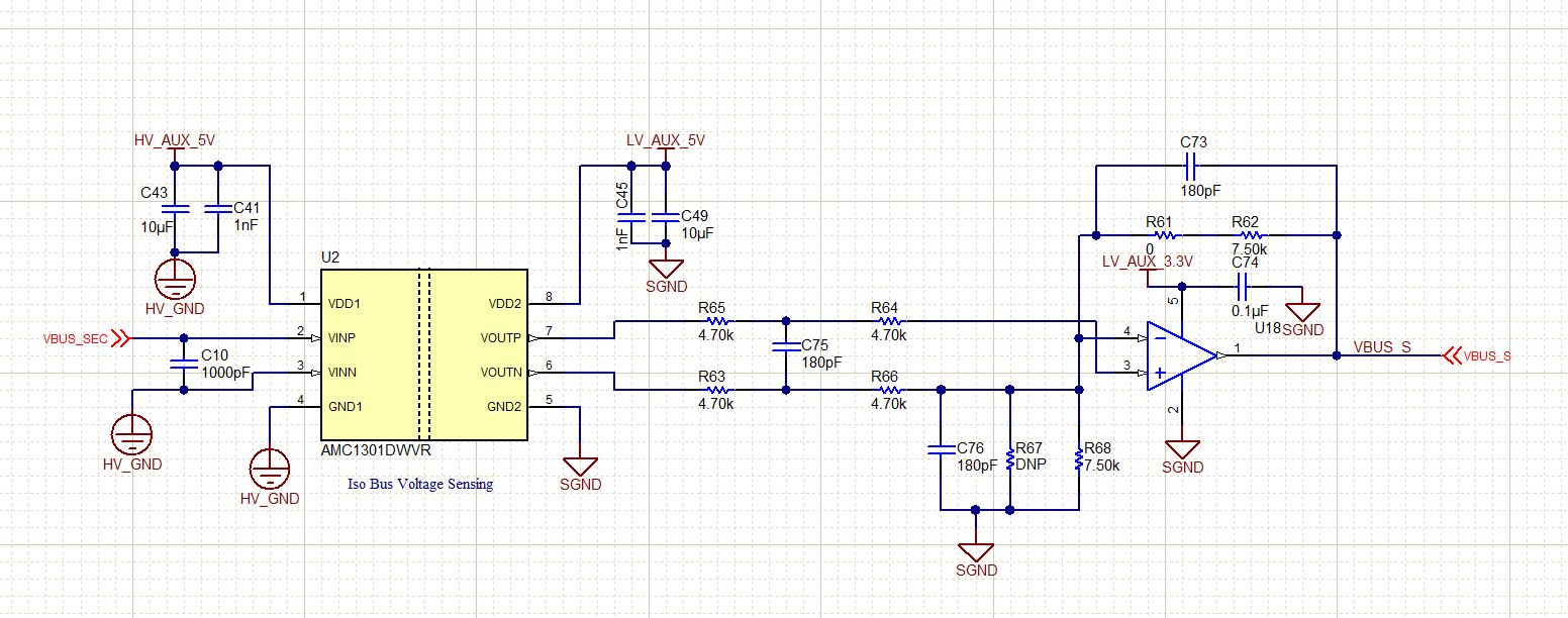
We are having problems with the reading of the ADC channel whta comes from the VBUS voltage level. And we have found two different versions of the accomodation signal circuit from VBUS point to the ADC B6 channel. The question is, what is the correct between these two schematics?
1) Circuit shown on the PDF of the TIDA-00951 section 6.3.1.7 Isolated Voltage Sensing: http://www.ti.com/lit/ug/tidud04/tidud04.pdf

2) Circuit shown on the SCHEMATIC of the TIDA-00951 Sheet 3, and for that, the final ALTIUM project and physical PCB: http://www.ti.com/lit/df/tidrr65/tidrr65.pdf

We are reading always in Code Composer the same value in bits (Saturation): 4095 no matters the voltage in the pin VBUS of the power circuit.
- Regarding the last issue about the VBUs signal conditioning with the AMC1301 and the OPA276 circuit, both versions (TIDA-00951 and Altium files from your product website) are wrong.
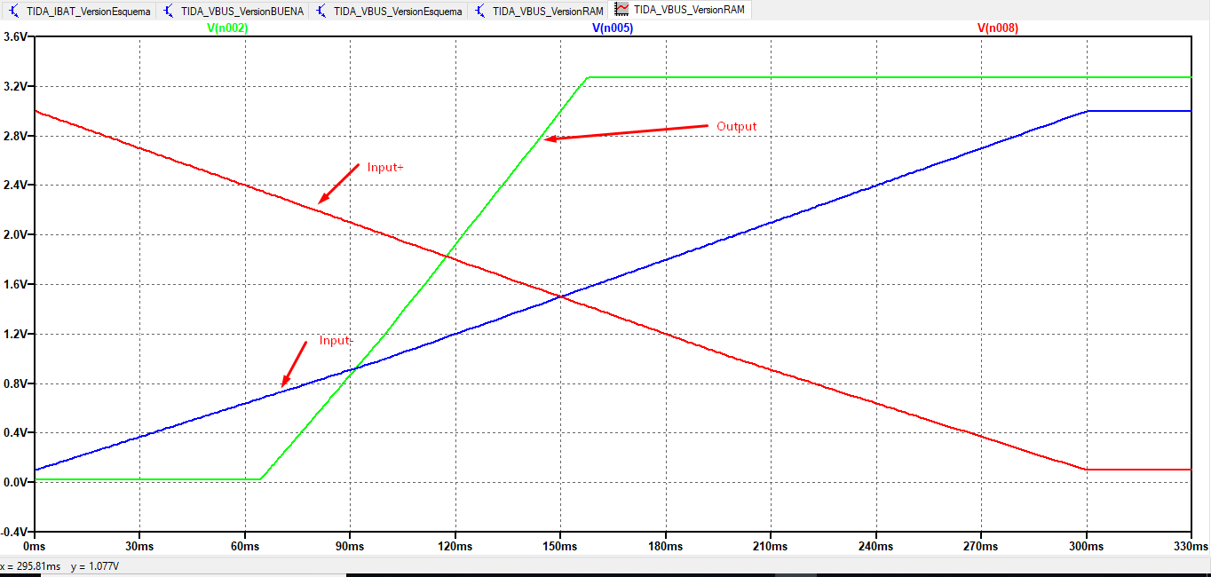
We have simulated both versions of the circuit in LTSpice and none of them works as espected, so we have searching on different application notes related to the AMC1301 and OPA376 as an isolated signal conditioning and we have found the right configuration, which works fine in LTSpice. This circuit is shown below:

- Because we have the manufactured PCBs and the software already running in the LAB, your proposal needs a Hardware modification in the PCB project, etc. Anyway, your circuit proposal doesn't work in simulation as we spects for that signal conditiong of VBUS.
- We have implemented in the PCB another version connecting +1.2V offset voltage in the R68 pad. And now we have got good results at testing LAB:


Please, let us know your thoughts about it.
Have a nice day,
Regards,
Guillermo Perez