Hi Teams,
I have a questions in PMP20195 reference design. how is D3/D10 purpose in this schematic? If I remember correct, if this power supply is two switch forward converter, D3/d10 is necessary. I double check the schematic, which is two switch flyback power supply. Can you help to understand the D3/D10 purpose?
By the way, the transfromer core is PQ32, right?
Tks, teams. 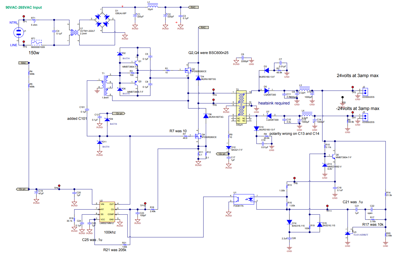
Regards,
Xiaobing (Eric)