This thread has been locked.

If you have a related question, please click the "Ask a related question" button in the top right corner. The newly created question will be automatically linked to this question.

TIDA-01371: Follow the reference design, shall I remove those components which are canceled in tiduci3a.pdf, but still in Altium?

Part Number: TIDA-01371
Other Parts Discussed in Thread: TPS7A47, TPS7A33, CSD19533KCS

Hello TI,

I am confused in following your TIDA-01371 ref. design. Could you please help me to understand this design correctly?

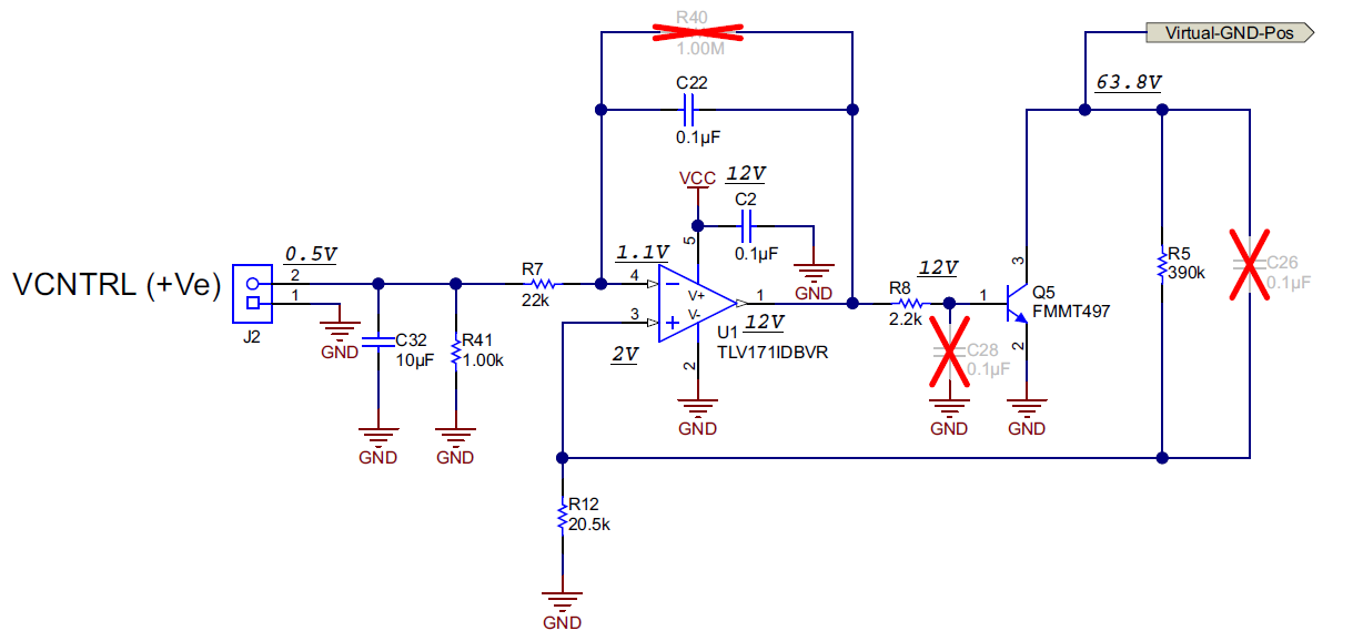
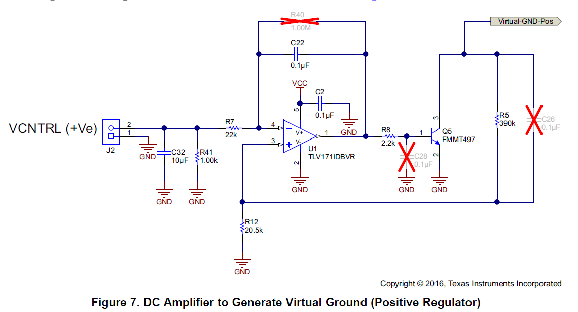
1. R40,R38, one 1MΩ shunt resistor is in parallel with a feedback cap of a opamp as an integrator, Both are cancelled with a red cross in datasheet, but are still in the schematic of Altium

What is the purpose of these 1MΩ resistor? the bleeding resistor to reset the integrator? Shall I keep them on board?

2.  C26, C28  are also cancelled in the datasheet,

What function do they play in circuit, why are they cancelled in datasheet? Shall I keep them on board?

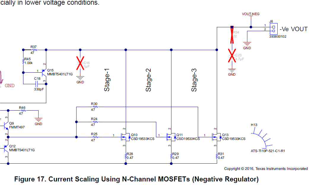
3. C16 and C7 are dual caps in the symmetrical design, why only C16 is canceled in datasheet? For simulation temporarily?

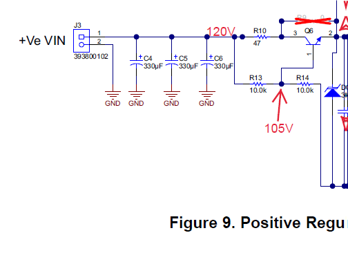
4. R34+C23 and R35+C24 are both the Zobel network. Why R34+C23 is canceled in datasheet? For simulation temporarily?

5.  R36 and R9 are zero Ω . The shorted BJT Q8 and Q6, which control the input voltage of those LDOs. If they are cancelled for other temporary purpose, why they appear in the schematic of Altium?

These are all my questions. 

Looking forward to your answers.

  • Hello Wallace,

    Thank you for your interest in TIDA-01371. Please find my answers below:

    1) R40 & R38 simply introduce a DC negative feedback. If you have space in your layout, I would recommend to keep the footprint of the resistors.
    2) C26 & C28 were kept to see if we need to filter out any noise during the development. While testing, you can always try different cap values and see the filtering operation.
    3) Both the LDOs have different architectures, so their stability will vary accordingly. While testing the design, we found that TPS7A47 was stable with C7 and TPS7A33 was stable without C16. I recommend that you keep the same configuration as the schematic.
    4) Same answer as point 3. During the testing, TPS7A47 was stable with Zobel network that is why mounted.
    5) R36 & R9 were used temporarily. You can remove those in your design.

    In short, these are reference schematics and we keep DNPs to test different scenarios during testing.

    BTW, what is the application you are working on? How is floating +Ve/-Ve LDOs are useful in your application?

    Thank you.

    Regards,
    Sanjay R. Pithadia
  • Hello Sanjay,

    Thank you very much for your patient and detailed reply!

    I am going to power it one and see what would happen.

    BTW, what does "DNP" stand for?

    The underlying application is to power a pulser for ultrasound transmission.

    Best Regards!

    Wallace


  • DNP means "Do Not Populate" on board.

    Regards,

    Sanjay R. Pithadia

  • Hello Sanjay,

    Today I tried to pull 1A current at 10V from the positive part, while the positive circuit is driven by +64DCV.  A few seconds later, the circuit failed and the +64DCV source went into constant current mode.  Then I unloaded the load resistor and re-powered this circuit, suddenly suspect  Q5 BJT was burnt. 

    The control part key voltage is provided on top of Figure 7 of tiduci3a.pdf.

    Doesn't this circuit support a continues current output, even the constant current is a fraction of the rated 6A?

    According to the voltage value measured at the circuit nodes of Figure 7, can we conclude that Q5 was burnt to be broken-circuit?


    I wish you could guide me in getting over this circuit and many thanks in advance!

    Best regards!

    Wallace

  • Hello Wallace,

    The circuit should work for continuous Iout of 1A.

    For 0.5V input, the virtual ground point should be at 10V. Where did you get 64V from?

    The virtual ground point is automatically generated.

    Which transistor did you use for Q5?

    I am attaching TINA simulation file which you can try before testing the actual circuit.

    Regards,

    Sanjay R. Pithadia6470.Positive-LDO-Virtual-GND.TSC

  • Hello Sanjay,

    That 64V was the input voltage of TIDA-01371 and the output was trimmed to be 10V. Under such condition, 54W was dumped into the  positive part of TIDA-01371 when 1A current was pulled out.

    Is this power dissipation too much for TIDA-01371?

    After the circuit failure, the virtual ground became 64V too. Therefore, I guess Q5(FMMT497) may be broken. 

    According to your knowledge, is my guess right?

    Best Regards!

    Wallace

  • Hello Wallace,

    54W is too much. The circuit will not be able to take this high power continuously.

    1) Is your schematic same as TIDA-01371 schematic?

    2) Is your layout same as TIDA-01371 layout?

    3) How many FETs have you connected in parallel with the LDO?

    4) Have you connected heatsink to the FETs?

    5) I would recommend to start with lower input voltage. Try with 25V at input, set the virtual ground at 10V and check the performance.

    Regards,

    Sanjay R. Pithadia

  • Hello Sanjay,

    1) Is your schematic same as TIDA-01371 schematic?

    A1: Yes. They are same.

    2) Is your layout same as TIDA-01371 layout?

    A2: 99% similarity.

    3) How many FETs have you connected in parallel with the LDO?

    A3: CSD19533KCS *3 in parallel with the LDO of both polarities.

    4) Have you connected heatsink to the FETs?

    A4: Not, yet.

    5) I would recommend to start with lower input voltage. Try with 25V at input, set the virtual ground at 10V and check the performance.

    A5: Thank you for your advice. I am doing so.

    Best Regards!

    Wallace