I am referring TIDA-01505 for designing similar circuit. Only difference is the output voltage is 12V instead of 15V.
Below are the specification:
- Input voltage range = 40Vdc – 1000Vdc
- Auxiliary voltage 1 = 20Vdc
- Auxiliary voltage 2 = -5Vdc
- Output voltage = 12V
- Output power = 48 Watt
- Switching frequency = 140kHz
- Max duty cycle = 85%
I have few question & doubts regarding the reference design TIDA-01505. Request you to please help in understanding design better:
- In the reference design calculation of TIDA-01505 for startup circuit below are the observation and wanted to know how does it worked for you.
- values arrived in the equations (37) for startup current is wrong. Startup current should be 102.6 mA but mentioned as 0.103mA.
- Hence the collector resistor calculation of Darlington Pair should not be 314Kohm (as written in Equation (38). Rather it should be 314Ohms
- In the equation (39), IC_max =3.1A is calculated correctly (by taking 314ohms as said in the point (b) above).
- Ic_max is specified in the datasheet of Darlington Pair transistor STP03D200 is 100mA. But calculated Ic_max in point (C ) above is 3.1A. How does transistor survive this huge current.
- In equation (40) the power dissipation is calculated with 3.1mA which is wrong it has to be 3.1A. Hence power dissipation comes hypothetical for a 60W power supply design.
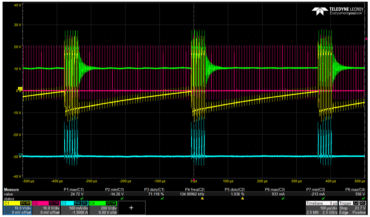
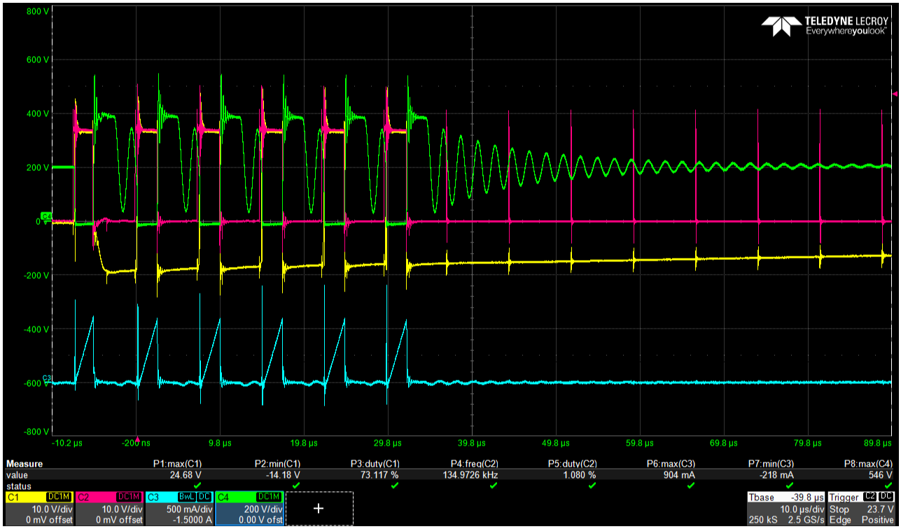
Can you please share the calculation and values of startup circuit which has worked for you in lab testing described in figure (14) in the reference design TIDA-01505
Does startup circuit works for entire range 40V – 1000V or it works for a specific input voltage.
- With the external voltage source (VDD) of 16V @ >80mA MOSFET C2M1000170D works fine. But for current<80mA, MOSFET is loading the VDD supply and PWM controller goes to UVLO mode and hence disabling PWM. We tried to increase the VDD capacitance from 22uF to 270uF. But it didn’t help.
- We have seen few SiC MOSFET - C2M1000170D failure and observed Gate and Source showing short. Did you also faced similar issues. At full load conditions & higher voltage ~ 950V SiC MOSFET has failed. Can you help in resolving this issue.
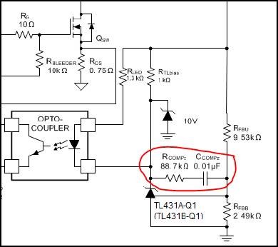
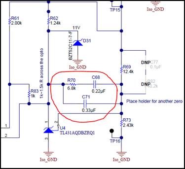
- In the datasheet of PWM controller UCC28C43-Q1 transfer function arrived in equation (53) doesn’t include the type 2 compensation (see below image) while the reference design TIDA-01505 include type 2-compensation. Can you provide the transfer function to check the stability.
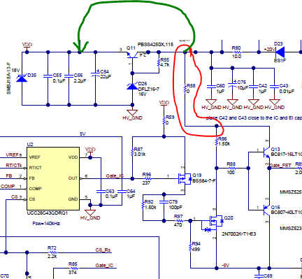
- In the below image, VDD connection to Totem pole is given directly from unregulated voltage from Transformer Auxiliary winding. Is this purposefully done as shown in below figure (red color) . Or it should have been connected to regulated supply as shown in figure(green color).
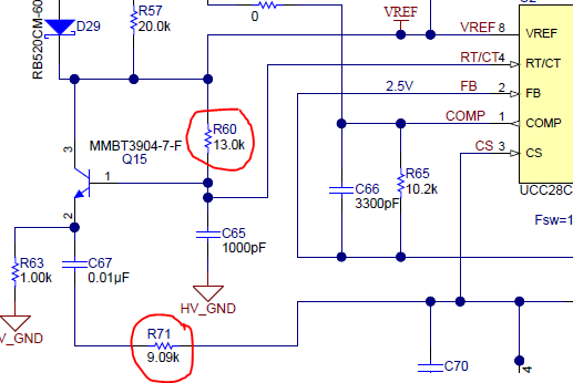
- In the reference design TIDA-01505 under the slope compensation network, Rramp (R71=9.09kohm). But its suggested to choose this resistor value higher than the value used in RT resistor (R60 =13K) as per section 2.3.11.1 (between equation 54 & equation 55). Refer the below image:
- We have chosen EF25 (N87 grade) transformer for the design to meet the board dimension requirement.
Below are the information on EF25 transformer:
|
Number of turns |
AWG/strands |
Effective AWG |
Turns ratio wrt primary |
Inductance (uH) |
|
|
Primary |
45 |
32/10 |
22 |
990 |
|
|
Secondary |
3 |
32/60 |
14 |
15 |
4.45 |
|
Auxillary1 |
6 |
32/6 |
26 |
8 |
17.60 |
|
Auxillary2 |
2 |
32/6 |
26 |
32 |
1.96 |