This thread has been locked.

If you have a related question, please click the "Ask a related question" button in the top right corner. The newly created question will be automatically linked to this question.

TIDA-00792: Why thermal calculations is far away from the real results?

Part Number: TIDA-00792
Other Parts Discussed in Thread: BQ78350-R1, BQ78350

Hi all,
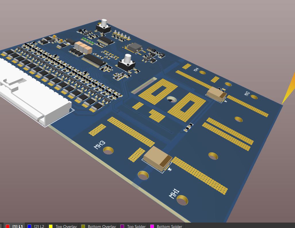
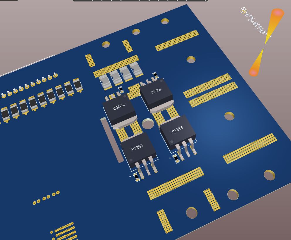
I just design a new BMS based on many reference designs with my own requirements, considering TIDA-00792 in "3.2.2.2 Thermal" when making the calculations based on total P_losses = 2.12W but with one FET everything goes right but as I think every MOSFET will share P = 0.54W (assuming equal power-sharing) so calculating based on P= 0.54W the result is far away from real value! why?


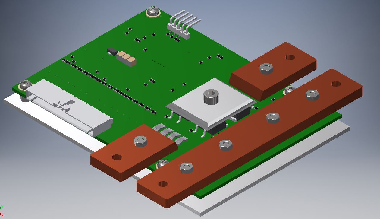
another question in my design the 4 FET share 
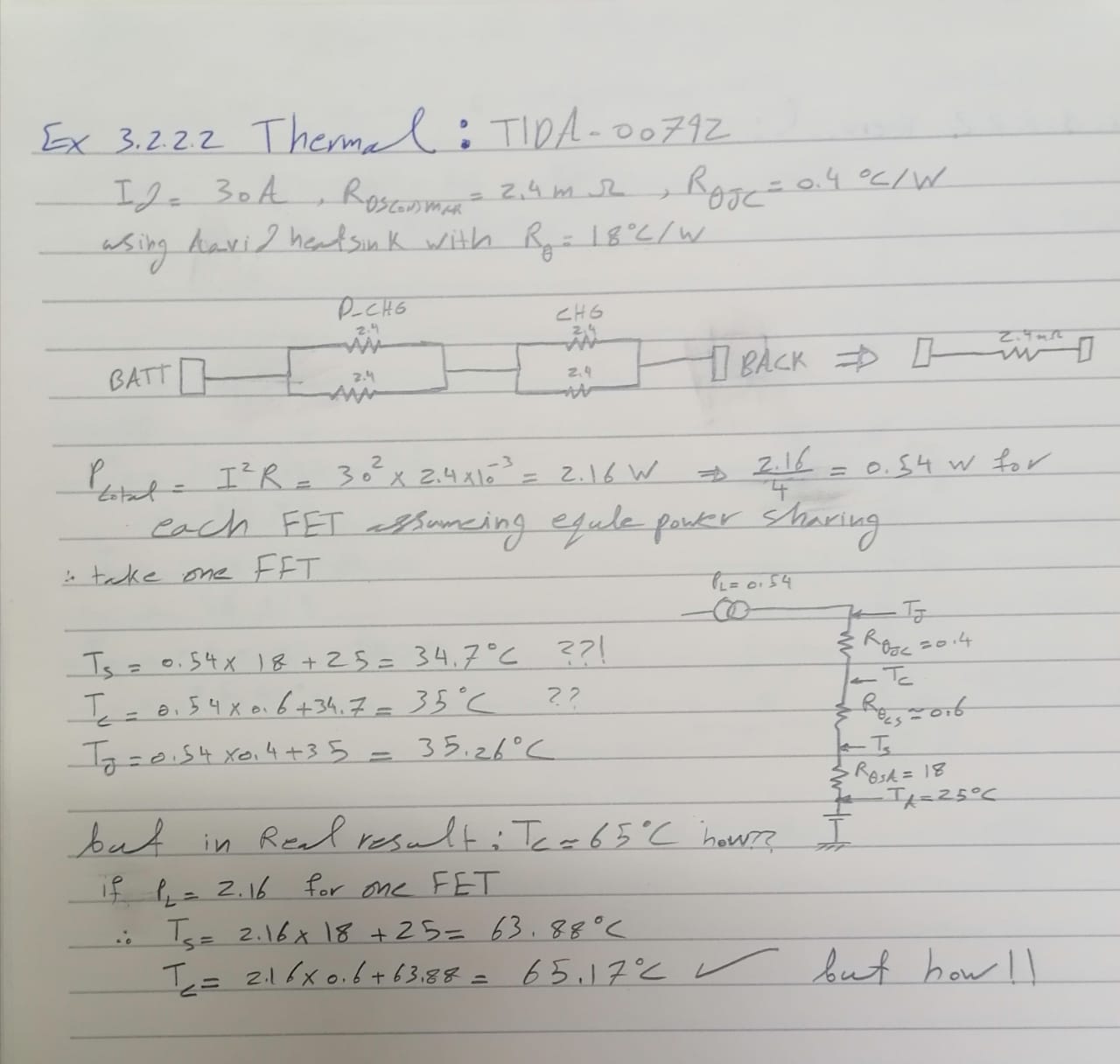
the same heat sink and total P_losses = 24W, it's correct to parallel the Junction-to-case thermal resistance, right?

  • Hi Rashad,

    Thanks for the inquiry. I did not work on this reference design and will send this over to the team that did after I respond. Your assumption that the FETs will share power is reasonable because of the positive temperature coefficient of rds(on). A few things to keep in mind:

    1. Because rds(on) increases with temperature, you need to take that into account in your power loss calculation. See Figure 8 in the datasheet.
    2. The heat sink relies on airflow for cooling. Do you have airflow in your system?
    3. Your assumptions for RthetaCS may be too low.
    4. You could be getting heating from other components near the FETs or thermal coupling between the FETs

    Please see the following blog on how TI specs and tests thermal impedance of our packages:

  • Hi John

    Thank you for your help, so you say that it correct to calculate based on  P_losses = 0.54W for each FET, not 2.16W? 

    But why when calculating based on P_losses=2.16W for each FET the results are found as in real test? it's a coincidence? 

    And for your points: 1- I take the Max. Rds(on)=2.4 

                                     2- No I don't have, but the heatsink is also rated at natural cooling (# 573300D00010G -> Thermal Resistance @ Natural:18.00°C/W).

                                     3- the RthetaCS value is very law mostly from 0.2 to 1.5 based on the interference compound.

                                     4- I don't think there is any heat source that makes this result very far.

  • Any help? Any idea?

  • Hi Rashad,

    I have to apologize. I sent this over to the team I thought had done this design to get their input and they have not responded. To address the power loss, my understanding is you either have the charge FETs on when charging the battery or the discharge FETs on when discharging the battery. Assuming the current divides equally between the two parallel FETs, the total conduction loss = I^2 x rds(on)/2 with each FET dissipating half of the total conduction loss. If your current is 30A, then the total conduction of two parallel FETs = (30A)(30A) x (2.4mOhm/2) x 1.3 (assuming 75C case temperature) = 1.404W and each FET dissipates about 0.7W.

    With regards to the thermals. The primary path for removing heat from the D2PAK is thru the tab. The thermal impedance TI specs in the datasheet is junction to bottom (tab). The thermal impedance thru the top of the plastic case is much higher. It is not specified in the datasheet but from thermal modeling, we estimate it is ~30C/W. Even if the heatsink makes direct contact with the plastic case, it's not a very low thermal impedance path. The heatsink looks like it solders down to the PCB. The primary thermal path will be from the tab, thru the PCB copper and into the heatsink. I'm thinking that is a lower thermal impedance than thru the top of the case to the heatsink. The total thermal impedance will be the parallel combination from junction-tab-PCB-heatsink-ambient and junction-top-heatsink-ambient. Please review and let me know if you have any additional questions.

    Here's a blog with more details on how TI specs thermal impedance of our FETs.

  • Hi John,


    Thank you really for your help.
    I misunderstood that the thermal impedance TI specs in the datasheet is the junction to bottom (tab) and not junction to top, again thanks a lot! and because of this, I change the thermal design completely and I will upload photos for PCB design so you and everyone can give me any good advice to improve the design layout and I will be grateful to him also.

    A small note from my understanding from (3.1, page:16, bq78350-R1 Technical Reference) that the two FET will be switched on either in charging or discharging case to protect MOSFET and reduce the power losses inside the other FET(charge FETs when discharging)?

    And I found this and many others very helpful, so thanks to every one contribute and share his knowledge!

    e2e.ti.com/.../understanding-mosfet-data-sheets-part-6-thermal-impedance

    e2e.ti.com/.../optimized-thermal-design-for-three-phase-motor-drives-in-power-tools-part-1

    e2e.ti.com/.../optimized-thermal-design-for-three-phase-motor-drives-in-power-tools-part-2

  • Hi Rashad,

    That is correct - the BQ78350 has a body diode protection feature that will turn on FETs to protect them when significant current is flowing. This is important in a series FET configuration. 

    Best regards,

    Matt

  • Hi Matt,

    Thank you so much:)

    I upload the third version of the design so maybe you can take a look, I just remove the long high current path from PCB to be cost reduction and more stable design, any comment is very welcomed.

    *100A continuous discharge current 

    *200mA balancing current 

    *0.5A Pre-charge current

    *Low-side protection switching with allowing communication while protected.

    If the schematic is needed I will send it to you.

    Thanks in advance.

    Best regards,

    Rashad

  • Hi Rashad,

    The layout looks good to me. I'm not sure if John has additional comments on the FET portion, but it looks good to me.

    Best regards,

    Matt

  • Hi Rashad,

    Thanks again for your interest in TI FETs. Based on what I'm seeing in the pictures the layout of the FETs looks good to me.

  • Hi Matt,

    Thanks a lot man U+1F929 I really hope for more advice from everyone U+1F970 and I waiting for John maybe he can add some comments. U+1F917


     Best regards,

    Rashad

  • Hi John,

    I'm the one he needs to thank you and TI actually! 

    Now I will go ahead to testing and prototype stage xd>>


    Best regards,

    Rashad