


Part Number: TIDA-01627
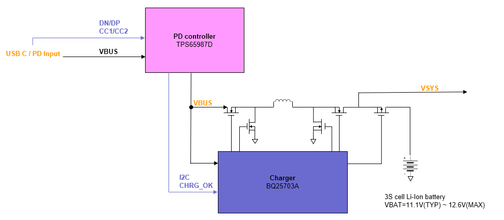
The picture above is my initial architecture.
I am going to use TIDA-01627 for input power architecture, and I have some questions.
1. Is SPI flash necessary or optional for TPS65987D?
- If the BP_NoWait and Configuration 3(datasheet 8.4.1) can meet my requirements, do I need external SPI flash?
- In addition, are the parameters of BQ25703A stored in SPI flash and written through the I2C of TPS65987D?
2. What’s the power path flow? It seems not the same for the reference schematic and the block diagram.
In TIDA-01627 schematic:
- The VBUS_C is transferred out of PP_HV via TPS65987D, and then connected to the BQ25703A input.
In TIDA-01627 blockdiagram:
- The VBUS_C is not connected to TPS65987D
I think I should follow the schematic instead of connecting VBUS_C to the inputs of TPS65987D and BQ25703A respectively.
3. Is it necessary to use 3.3 buck for power up TPS65987D in my architecture?
- It seems the device can be booted up internally by using VBUS input.
- if yes, can I use LDO to replace buck?
4. Any concerns if we don’t place TPD8S300? Is TVS appropriate?
Thanks,
Vic
