This thread has been locked.

If you have a related question, please click the "Ask a related question" button in the top right corner. The newly created question will be automatically linked to this question.

TIDA-00961: F280049

Part Number: TIDA-00961

My company is building 4 pieces of the reference PDC Design TIDA-00961, 1.6kW, High Density, GaN-Based, CrM Totem-Pole PFC Converter Reference Design.

We also purchased the LMG3410-HB-EVM and TMDSCNCD280049C daughter/controller cards to plug into the TIDA-00961 main board.

My question is whether we need to pre-program the TMDSCNCD280049C daughter card prior to being inserted into the TIDA board?

If pre-programming is required, what hardware and software do I need to accomplish the programming.

Bruce Crosley

  • Hi, Bruce

    Thanks for interesting this TI reference.

    TIDA-00961 is the digital controlled PFC which will need firmware inside.

    You need to install CCS tool in first,

    and then, download the tool of C2000Ware_DigitalPower_SDK, you will find the reference code in \ti\c2000\C2000Ware_DigitalPower_SDK_3_00_00_00\solutions.

  • Do I need any additional hardware (test board or docking station) to install the firmware?

  • Hi, Bruce

    all you need is the mother board and daughter board, F280049 cCard can communicate with CCS directly.

  • Problems with Open Loop test of TIDA-00961 GaN PFC

    B. Crosley – 21 Apr 2020


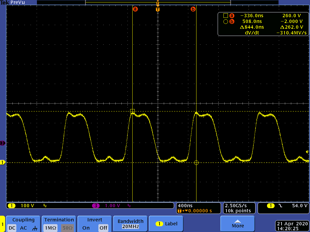
    Description: I am bringing up the TIDA-00961 Gan CrM Totem-Pole PFC Converter according to your TIDA-00961 Software Guide (File # TIDUDU4C) in open loop mode (build 1). On page 15, P3.5.1.6 shows Figure 7 as the Switch Node voltages I should get at 100Vdc Input and 333 ohm load output. It also states I should see about 122Vdc out. When I perform the open loops steps, I get the waveform below at J201 Switch Node 1. I also have 232 Vdc output (ton = 20) and the load is set at 330ma. When Looking at the LS Gate 1 signal (J204-2) and appears normal. The J204-1 HS Gate1 signal is initially “normal” but goes low when the input gets above approximately 50Vdc. The same is true for the other GaN FET pair (J209).

    Is the waveform below normal or is something not working properly (it does not look like Figure 7 in the Software Guide).


  • Hi, 

    This picture shows your GaN device not well turn on.

    Please check your power supply of GaN device and its driving input.