This thread has been locked.

If you have a related question, please click the "Ask a related question" button in the top right corner. The newly created question will be automatically linked to this question.

PMP8740: PSFB T4 Primary waveform looks strange at my PMP8740 board

Part Number: PMP8740
Other Parts Discussed in Thread: UCC28950

Hi ,

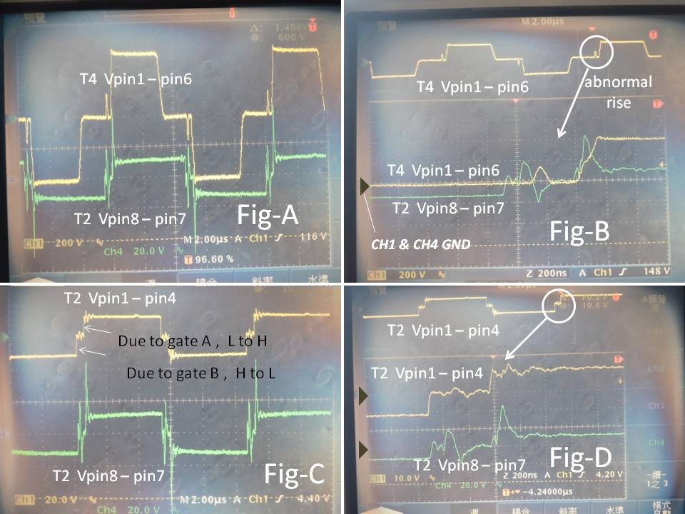
I had some finding , previously that I called a spike on T4 primary ( I labeled it as an abnormal rise then fall to 0V in Fig-B ) may not leakage ringing. 

 Fig-A, B, C, D as attached . from Fig C and Fig-D , I thought it is because T2 gate drive Vpin8-pin7  , gate B H to L make T2 

had 1st trial to turn on Q8 a little, but soon undershoot pull Q8 off at once , followed by  gate A L to H that really turn Q8 on . my waveform of T2 8-7 may or may not TI original design looks.

I change the R78 , or R71 and R76 for 2-4 times higher , resonant waveform ( Fig-D green ) always stay the same.

Furthermore , DC level of T2 Vpin1-pin4 waveform at Fig -C is weird to me , should C43  remove the AC content ? I use the same component value and exact T2 from TI BOM.  BTW, T2 Vpin6-pin5 is

more , not like T2 pin8-pin7  huge overshoot and undershoot.

Furthermore, T3 pin8-pin7 waveform is very clean , not ringing like T2 pin8-pin7 ;

Test at Vo~43V / 8A, PSFB X’former turn ration 28:5 ( PQ5050) , additional leakage inductor 10uh ( if I use 5uH, that abnormal rise peak became smaller ) .

If probe left node of T7 , and T4 pin 6 , it still similar to probe T4 pin 1 and pin 6 , a little bit time difference only.

the 2nd weird to me , when Q15 off , circulate current at  both Q15, Q16 stop , energy storage  at x’former leakage plus 10uH inductor should gave  a rising to 400V on Q8 source node  , but it just one peak rise then fall to 0v.   plus that , Q8 and Q9 never achive ZVS, even though at 43V/8A condition , they are hot.  I had also tried to short the leakage inductor , it only reduce the peak only .  

that gate drive waveform on Q8 is  really weird at my PMP8740 board . 
  • Hello Norman,

    I have few questions about your design: does it have the same specifications like the PMP8740, so 2KW nominal?

    I ask because 43V @ 8A is 344W, which is only 17.2% of nominal load. With 10uH shim inductor there is a minimum load needed in order to achieve ZVS.

    Please refer to UCC28950 EVM calculation tool to derive what is the minimum inductance you need to get ZVS in a programmed load range.

    Also the fact that you see spikes on the gate driving transformer voltage, in one transformer only, where ZVS is not active, might depend on the fact that the dV/dT is very high and you get noise in your scope. In order to double check that, please connect the isolated probe (must be isolated because we are talking about the floating driving section) shorted to the floating ground of Q8, which is the source of Q8, therefore connecting the ground and the tip of the isolated probe both on Q8 source. If you see spikes, then they are not real, because you should see zero.

    Regarding the gate drive transformers T2 and T3, are you using the parts 56PR3362? These transformer are behaving better compared to the original ones I used, which are the AF4779.

    Best regards,

    Roberto

  • Thank you Roberto,

    1) I use 10uH shim inductor , and I intend for 48Vbat at 20A design

    2) I always use differential probes at this board measurement

    3) I can adjust 10uH to decide when > certain load to approach ZVS, however I do have  concern on this abnormal

      ( to me , and it seems real and bother me ) voltage rise then fall on both condition when either gate B off --> gate A on , or  gate A off --> gate B.

    because I did not see similar on many others design .

    4)Herewith I attach 3 photos I measure today together with current probe ( Q8 drain to source direction )

    thank you for any advice from below ~ 

  • Hello Norman,

    According to the first screenshot, I see that the waveform of CH4 (V8 Vgs) has a spike up to +42V. This high voltage should already damage the gate of Q8. I am wondering how it can be that you have so high value of spike. Did you make the test I suggested, by connecting both scope terminal and its ground (isolated probe) to the floating node (source of Q8)? If you analyzed this waveform, did you see just zero volt continuous waveform or did you see also spikes? If you saw spikes, they are affecting your measurement. If, instead, you saw a continuous line, showing zero voltage, then theses spikes are real and dangerous. I can only explain these spikes by too high leakage inductance in the transformer T2 or too high value of resistor R73 (higher than 10 Ohm).

    Did you use the same FET I employed, like IPP65R190CFD, or are they different?

    Thanks,

    Roberto

  • Hello Roberto,

    I use the same IPP65R190CFD , and also use 56PR3362 for all gate drive x'former. 

    Let me get another main PSFB transformer with lower leakage then try ( current one I need to test

    leakage when I have LCR meter , but I can tell its coupling may not good from the very fat  winding.

    maybe need to use copper foil for secondary, instead of existing big round  litz wire that far away from primary

    winding , it may cause poor coupling ( ie.,  large leakage )

    I'm not sure I catch your point  on tie isolated probe ground and scope ground to Q8 source ...

    I use the differential probe ( red tip and black tip , plus tip is isolated amplified to its BNC cable to the scope BNC )

    and I think it is what you mentioned an isolated probe. But scope BNC gnd = scope's chasis gnd = scope AC plug's earth gnd ,

    and I usually don't connect scope plug EARTH gnd  to ac outlet earth gnd,  due to sometimes when non isolated probe BNC gnd tie

    to AC primary circuit ( L or N) of DUT board will cause  ac outlet earth gnd short to L or N.  and I treat Q8 source is low impedance to L or N.

    that's also why I use isolated differential probe . so I am confused with if  scope BNC gnd been tied to Q8 source , whole scope chassis short

    to 400V - a low impedance to L & N , is this kind of dangerous set up ?  

    best regards

    Norman

  • Hello Norman,

    OK, I see you are using the same FET I employed in my design, as well as the gate drive transformer.

    Regarding the isolated probe tied to Q8 source I meant:

    Connect both red tip and black tip to the source of Q8. This way, the input of the differential probe should show zero on the scope. If you see spikes, they are not real, but just a noise current flowing from the switch node (*source of Q8) all the way back to the scope. This current can be avoided by winding the cable of the differential probe into a core (used normally for common mode choke).

    Best regards,

    Roberto

  • Hello Roberto ,

    I ties two tips to Q8 source and a flat zero voltage line , so that spike right after gate B turn off is real . 

    Yes, let me have another low leakage PSFB  X'former to try.

    Thanks!

    Norman