This thread has been locked.

If you have a related question, please click the "Ask a related question" button in the top right corner. The newly created question will be automatically linked to this question.

PMP20878: Auxiliary Supply vs. POE Supply

Part Number: PMP20878
Other Parts Discussed in Thread: UCC2897A, TPS2373-4EVM-758, TPS2373

Dear all,

are the test results for the PMP20878 only valid for an auxiliary supply (40-57 VDC on J3) or was the board tested with a POE supply (IEEE 802.3bt) as well?

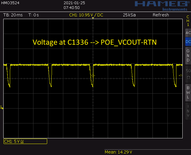
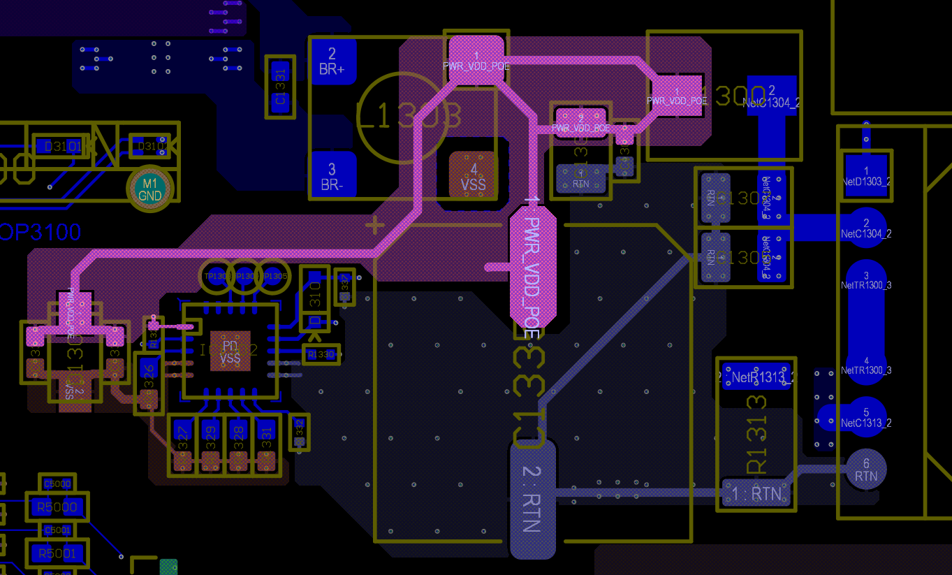
We designed a circuit which is almost equal to the PMP20878 evaluation board (24V/3A output). If we use the auxiliary supply, the PWM controller and the active clamp-forward converter work as expected. But if we plug in the ethernet cable the circuit does not work properly. We can share the schematic and some scope pictures to explain the problems in detail.

Since the PMP20878 evaluation board is not for sale we are not able to check if the circuit really works for POE operation.

Best regards,

Valentin

  • Dear all,

    please see the schematic of our POE circuit and some scope pictures attached.

    Main differences between our circuit and the PMP20878 evaluation board are:

    • M12 connector 21033814827 from Harting with integrated magnetics (J3000)
    • Dual MOSFET-based bridge recitifier from Microsemi (D3000)

    Schematic_POE.pdf

    We have captured the following scope waveforms:

    • Startup voltage of VSS-RTN

    • Voltage at C1336 --> POE_VCOUT-RTN

    • Voltage at C1337 --> POE_VCIN-RTN

    • Voltage at C1325 --> POE_SS-RTN

    At first, we checked the behavior of the active clamp-forward converter without the PD interface TPS2373-4 (IC1302). Therefore we used two voltage sources to generate PWR_VDD_POE = 54 V and POE_VCOUT = 12V. The connections between TPS2373-4 (IC1302) and UCC2897A (IC1300) have been disconnected for this test (desoldering of R1330 to cut POE_SS, PCB track for POE_VCOUT between IC1302 and IC1300 destroyed). This part of the circuit works as expected, the converter generates 24V at P24V_POE with no extra load attached (the only load is the DC-DC converter U1200).

    Secondly, we measured the behavior of the whole POE circuit. As POE injector we used the 561495 from Intellinet (95 W port, IEEE 802.3bt conform). We soldered LEDs on the testpoints TP1303 (TPH) and TP1304 (TPL) which were blinking all the time. This behavior can be seen in the second scope waveform of POE_VCOUT-RTN. The voltage PWR_VDD_POE is equal to 54 V in this setup.

    What is most confusing to us is the voltage waveform of POE_SS-RTN (voltage at C1325). The periodical charging and discharging of the capacitor prevents the circuit from operating in the right way. This voltage waveform can be observed without the resistor R1330 (no PG signal from the TPS2373-4).

    The voltage at R1328 (AMPS_CTL output of TPS2373-4) is 0 V in this case. There are no periodical voltages pulses as in the datasheet (or as in the evaluation board TPS2373-4EVM-758).

    Troubleshooting:

    • Changed L1302 (744045102 from Wuerth --> 1 mH / 70 mA / 30 Ohm) to 74404054102 (1 mH / 200 mA / 6 Ohm) as in the PMP20878 evaluation board (there: L6)
    • 100 uF electrolyt capacitor added to pins 13, 14 of UCC2897A as in the PMP20878 evaluation board (there: C103)
    • R1333 desoldered (disconnected pin 2 of TPS2373-4 from optocoupler)
    • R1330 desoldered (disconnected PG of TPS2373-4 from SS/SD of UCC2897A)

    None of the above changes improved the behavior of our circuit.

    Therefore, we cross checked our board with the TPS2373-4EVM-758 evaluation board to validate the electrical performance of our M12 connector and inpute bridge. We desoldered the common mode choke L1303 on our board and L10 on the evaluation board (L10 is the same on PMP20878 and TPS2373-4EVM-758). We connected the soldering pads of the common mode chokes with the other board as follows:

    • TPS2373-4EVM-758 (RJ45 and discrete input bridge) --> cable from soldering pads 2 and 3 of L10 to soldering pads 1 and 4 of L1303 on our board --> circuit on our board
      • Our board does not work even with the input circuit of the evaluation board.
    • Our board (M12 and dual MOSFET-based bridge rectifier) --> cable from soldering pads 2 and 3 of L1303 to solderings pads 1 and 4 of L10 on TPS2373-4EVM-758 --> circuit on evaluation board TPS2373-4EVM-758
      • The evaluation board still works with the input circuit of our board.
    From this we can conclude that the false behavior of our circuit is not justified by a different input connector or input bridge. There must be a false wiring of TPS2373-4 and/or UCC2897A in our schematic.
    We would be grateful if someone can double check our schematic with the PMP20878. Is the schematic of the PMP20878 correct or is there a newer revision which has not been published yet? It looks like the PMP20878 has additional components soldered to the board (see the following image).
    Best regards,
    Valentin

  • Valentin,

    Yes, this board has been tested with a PoE input.  It is the same PoE circuitry as the TPS2373-4EVM-758.  There is also a 12V output version.  All have been used in various projects.

    The list of drawings on the web says the BOM is Rev A and the schematic is Rev B.  If you open the actual documents, they are both Rev C, which are the latest.  The above photo is a Rev A PCB modified to Rev C.

    I checked your TPS2373 and UCC2897A circuits and did not see any errors.

    On the TPS2373 you have four 100nF capacitors between POE and VSS, C1331-4.  The IEEE specification only allows 120nF total capacitance on the input up to the PD switch.  Three of these capacitors should be removed and replaced with lower value capacitors so that the total capacitance is less than 120nF.  I put the 100nF cap close to the TPS2373 and make the other capacitors 1000pF.

    Is there any load on VCOUT besides that shown on the PMP20878 schematic?  It looks like something might be loading VCOUT.

    Please reply again if removing the capacitors does not solve your problem.

    Thanks,

    David

  • Dear Mr Strasser,

    thank your for your quick reply!

    We have desoldered three of the four capacitors but the circuit is still not working properly.

    You can see the routing of the PWR_VDD_POE plane in the attached image. It seems like the power flow is incorrect.

    After the common mode choke we routed directly to the 100 uF electrolytic capacitor (C1335), to the inductor (L1300) and to the input of the TPS2373-4 (C1332, D1309, C1333, C1334, IC1302). According to the TPS2373-4 datasheet the routing should be as follows:

    Is this our main error? Should there be an improvement if we desolder the 100 uF electrolytic capacitor (C1335) for debugging purpose?

    Best regards,

    Valentin

  • Valentin,

    The VDD bus is common so the connections shown should be ok.  The 100uF capacitor is connected to RTN whereas the other components are connected to VSS.  The hot swap FET is inside the TPS2373-4 between RTN and VSS.

    I had one of the other application engineers familiar with the TPS2373-4 check your schematic.  He did not find any errors except for the 4x 0.1uF capacitors.

    We are continuing our investigation.

    Thanks,

    David