


Other Parts Discussed in Thread: TMCS1101
Hi,
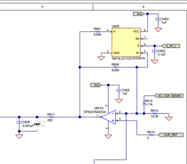
I'm working on adapting parts of the PMP40690 Reference design for a similar project and am having trouble figuring out the design intent of the AC Line Current Sense scaling circuit screen captured below:
I understand that the AC line hall sensor (U101) is supplied by 5V, centered at 2.5V and the goal of U601A is to scale the output voltage (AC_CUR_G) to the ADC input range which is 0 to 3.3V centered at 1.65V. It seems that U600 is being used as a firmware controlled gain setting to select between a gain of ~1.7 and ~0.85 with an offset of -2.58 and -0.46 respectively. In both cases, when AC_CUR_SENSE = 2.5V then the output is ~1.65V as desired. If my math is correct, when G_AC_I is LOW then the maximum allowable voltage swing for AC_CUR_SENSE (in order to ensure AC_CUR_G stays between 0 and 3.3V) is ~0.55V - 4.44V which corresponds to ~+/-38.8A. When G_AC_I is HIGH this is +/-19.3A.
My questions are the following:
Why is U101 supplied by 5V instead of 3.3V in this design? Per the datasheet for the TMCS1100A, the F.S. linear current range for this part with 3.3V supply is +/-29A which would cover the maximum peak input current of this reference design (~20A RMS or ~28.28A peak) albeit with a small amount of margin. Is the reason for powering this part on 5V that this amount of margin is unacceptable for some reason? Powering this part on 5V necessitates this otherwise unnecessary set of components.
Why is U601A supplied by 5V? Powering this part from 5V means that it is capable of outputting a higher voltage than the MCU input pin is rated to handle. R611 limits the current into the ADC input pin of the MCU to an extent but not to the +/-2mA continuous clamp current specified in the datasheet for the F280049 MCU. Why not power U601A from 3.3V and avoid this hazard altogether? U601A is rail to rail input and output so powering from 3.3V doesn't seem to have any disadvantages.
Why are the gains set to the values that they are? +/-19.3A and +/-38.8A seem almost arbitrary given the specifications of the design. Why not set the low current gain to say, 15A (since this is approximately the peak current when the converter is operating in 1 phase and 2 phase operating mode) and the high current gain to say ~+/-30A?
Can anyone provide more insight on why this was designed the way it was?
Thanks,
Joseph
