This thread has been locked.

If you have a related question, please click the "Ask a related question" button in the top right corner. The newly created question will be automatically linked to this question.

PMP12072: REV A board to the extended FETs board via the JP1 connector

Part Number: PMP12072
Other Parts Discussed in Thread: CSD19537Q3

Hi Guys, 

Good day. 

Could you help us to check our customer's design. We have attached here an schematic for your review. 

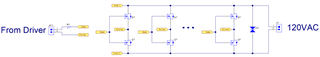
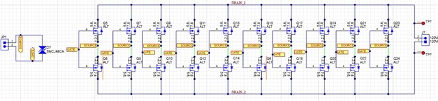
Our customer customized the board by designing a new PCB board where instead of just adding only Q3 and Q4 as shown in the original PCB board, they add several FETs and connect the Source (PIN 1, 2 and 3) and Gate (Pin 4) of the N-Channel MOSFETs via the JP1 connector. According to the original design of PMP12072 REV A, you can get more POWER or CURRENT by simply adding more of Q3 and Q4, therefore, they have added more of Q3 and Q4 and placed them onto a different PCB board. That way, it will have a smaller PCB that is easier to cool using a single heat sink. 

Q3 to Q24 on the schematic are N-Channel Power MOSFETs CSD19537Q3 (MOSFET MOSFET 100-V, N channel NexFET power MOSFET, single SON 3 mm x 3 mm, 14.5 mOhm 8-VSON-CLIP -55 to 150)

As you can see in picture 2 (let's call it the POWER STAGE), they can make more of the Power Stage PCBs to add either more Current or Power without the need to manufacturing another driver circuit (i.e the primary side with the transformer). Therefore, a single driver PCB board can drive several Power Stage PCBs (in picture 2) by connecting the GATE and the SOURCE of the N-Channel Power MOSFETS via the JP1 connector.

If you think it is not feasible, kindly let us know so our customer can find another way to add more current or Power for their project.

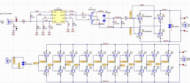
In addition to that. Could you also enlightern us about the frequncy used. is the frequency fixed? If not, how can you control the frequency? Do you think RT controls the output frequency, which means if they use a variable resistor, then they can tune the frequency. 


Thank you in advance for the support. 

Best regards,

Jonathan

  • Hello Jonathan,

    Yes, this is a fixed frequency part and the “RT” pin controls the switching frequency, which is currently set to 200KHz. This frequency is specifically chosen to work with the PA0173NLT isolation transformer. I don’t recommend changing it.

    Regarding the original question about having a single driver controlling banks of FETs: this should be fine, except due to the larger amount of gate capacitance introduced by so many FETs, the turn-ON and turn-OFF times of the FETs will take longer.

    Also, make sure that the output bank of FETs are connected to the same load, not different loads. The transformer provides isolation from the control input to the secondary-side load. If multiple loads are to be used, I would recommend using separate control units (i.e. separate push-pull drivers and transformers) for each load.

    The schematic shows a 120VAC on the load side where the FETs will be switching. If this is true, I highly recommend using FETs with a drain-source voltage rating of at least 250V. The reason for this is that the peak voltage the FETs will encounter can reach up to 190V. This also means that the bi-directional TVS diode rating needs to be changed to a higher value, maybe also a higher power rating.

    Finally, the schematic also shows the TVS diode in the customer’s new “Power Stage” board being connected between the Gate and Source. This is incorrect. Please connect the TVS diode (with the new, correct ratings) between Drain1 and Drain2.

  • Hi Hrag,

    Our customer have received your anwser and appreciated your support. I have reposted their feedback here. 

    "As suggested, I would like to ask if the following will answer the risen query regarding the original question about having a single driver controlling banks of FETs that in so doing, a larger amount of gate capacitance will be introduced by so many FETs, that the turn-ON and turn-OFF times of the FETs will take longer, therefore, if I put a 1 kOhm at the gate of the FETs, that should improve the efficiency by lowering the gate capacitance drastically. Lastly, how comes the source is not connected to the GND? I was thinking of using a 10 kOhm on the source of the FETs then connect it to the ground."

    Attached schematic for reference:

    Schematic.zip

    Looking forward to your answer. Thank you.

    Best regards,

    Jonathan

  • Hello Jonathan,

    There are a few incorrect connections in the attached schematic that I noticed on JP1.  I went ahead and drew a schematic to show you how the "Power Stage" board needs to look.

    The gate resistor does not need to be that high.  This gate resistor will not change the steady-state efficiency.  1 ohm is actually good.  If anything, the larger the value of this gate resistor, the longer it will take the FETs to turn ON and OFF and may generate more power loss (i.e. heat) during the ON->OFF or OFF->ON transitions.  Please see the attached schematic I drew, at the end of this post.

    Regarding the sources being connected to GND or not:  the "Power Stage" has no GND.  It is actually floating.  The only GND in the circuit is the isolated primary side of the driver where the 12VDC is connected.

    Another note I would like to make is that the SSR should not be connected to a transformer winding.  This will short the system.  Maybe this was only placed as a notation???  I hope so.  The two SSR output terminals need to complete a circuit, so it needs to be placed in series to the AC circuit, in order to open or close the loop.

    Finally, the voltage rating of the FETs are not visible, but as I mentioned in my previous post, the FET drain-to-source rating needs to be 250V rated or higher, to be safe.