This thread has been locked.

If you have a related question, please click the "Ask a related question" button in the top right corner. The newly created question will be automatically linked to this question.

PSPICE-FOR-TI: PSPICE

Part Number: PSPICE-FOR-TI
Other Parts Discussed in Thread: LMG5200, BOOSTXL-3PHGANINV

Hello. Help me.

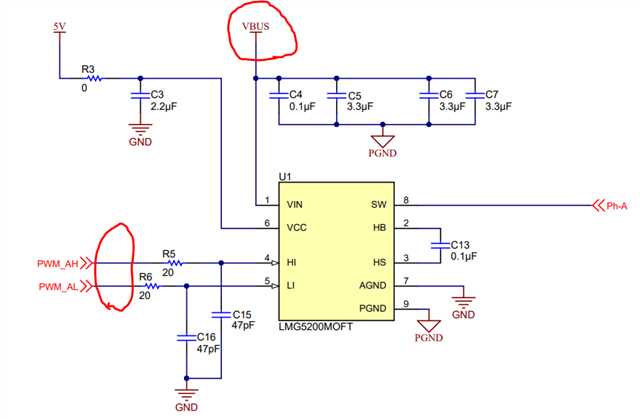
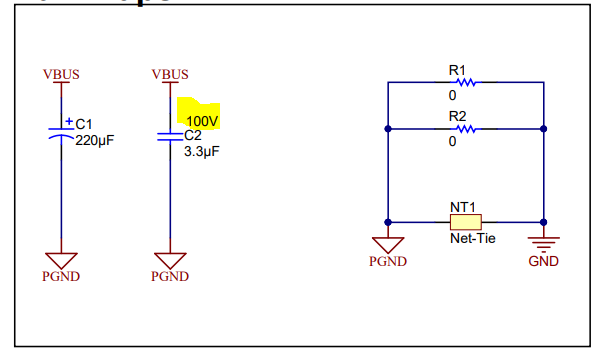
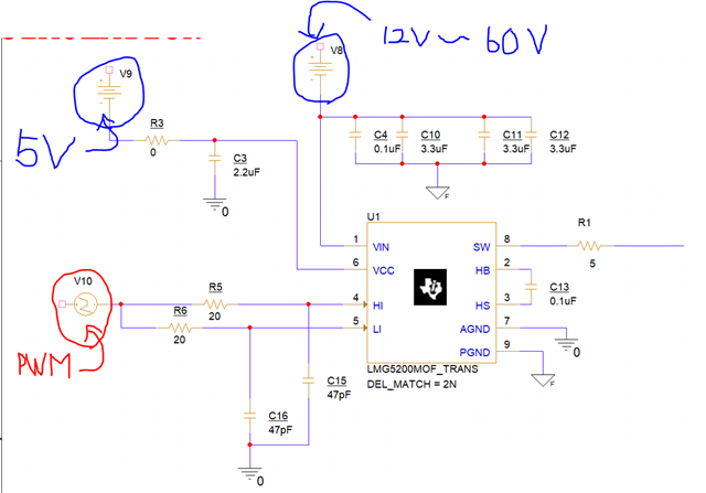
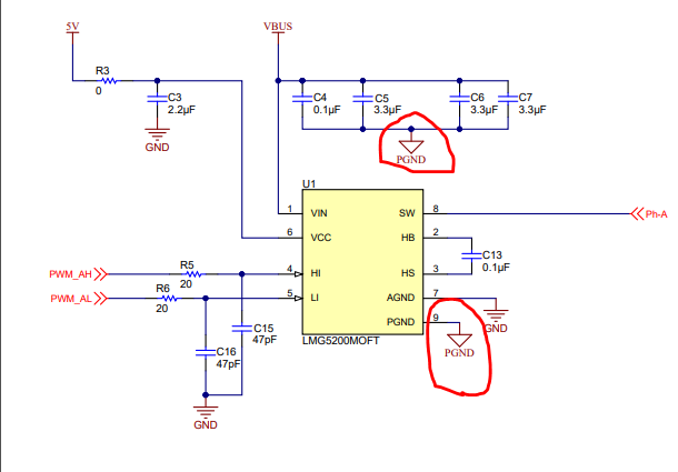
This is a 100V schematic of the LMG5200 of the BOOSTXL-3PHGANINV substrate.

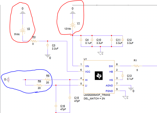
I want to analyze this circuit, but PSPICE has only 80V of LMG5200, so I want to create a circuit as shown in the image above.

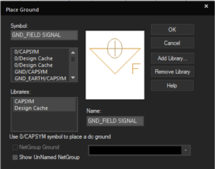
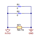
So how do you make PGND in the red frame of the image on PSPICE?

Best regards..

Tosi

  • Hi Tosi, 

    I believe PSPICE gives the option to use different ground symbols under Place -> Ground.  You can use these and then connect them together on the schematic. 

     The BOOSTXL-3PHGANINV uses these two grounds to separate the signal ground from the noisy power ground. In the schematic, the PGND and GND are tied as shown below:

    Regardless, for simulation purposes, different grounds are not required to be used to create a functioning system. It will have no impact on the simulation.

    Best Regards,

    John

  • Thank you very much for the reply.

    Now, regardless of the purpose of the simulation, you don't need to create a GND system. Because it does not affect the simulation.

    Another question.

    When simulated the circuit as shown in the image above, I think that it will not work unless the power supply is placed in the red frame.

    Is the VBUS in the red frame above a 100V power supply in the image on the right?

    What is the power supply of the left red frame?

    As I mentioned last time, this circuit is boostxl-3PHGANINV.

    I'm sorry for the confusing sentences. Thank you and point out.

    Tosi.

  • Hi Tosi,

    The VBUS voltage can range from 12V to 60V, as that is the voltage the inverter is rated for. The "100V" is referring to the voltage rating of the 3.3 uF capacitor between VBUS and GND.

    Please let me know if I understood your question correctly.

    Best Regards,

    John

  • Hi John thanks for replying.

    Then, as described in the first image, it is okay to say that the value between 12V and 60V is good.

    Then, the question is, is the symbol of the power supply correct in the second image?

    Eventually, PWM will be input to this circuit to observe the strained waveform. I don't ask many questions at once. However, I will ask you questions little by little, so thank you for your answer. I'm waiting for a reply.

    Tosi.

  • Hi Tosi,

    Those are the correct power supply symbols to be used for the VIN and VCC pins. However, the connections are not correct - the positive end of the supplies must be connected to the pins and the negative end should be referenced to ground. 

    Additionally, you will need two complementary PWM signals for the HI and LO inputs. There will be shoot-through in the half bridge if the same signal is used for both HI and LO.

    Best Regards,
    John 

  • Thank you for your reply.

    I also tried to connect GND by correcting the connection between the VIN pin and the VCC pin in the image above. Is this the correct answer?

    The blue frame is currently under production because it inputs a PWM source. Do you want to place GND here as well?

    Last time, John said, two auxiliary PWM signals are required for the HI and LO inputs. If both HI and LO use the same signal, a shoot-through occurs in the half-bridge. I would be happy if you could tell me more about .

    Thank you very much, really always.

    Tosi.

  • Hi Tosi, 

    Yes, those are the correct GND connections that are needed to bias the VIN and VCC pins.

    The PWM signals in your schematic are currently connected to each other. This will cause a problem because the high-side and low-side FETs will be turned on at the same time, which is not desirable for any switching power supply topology. 

    Please refer to the LMG5200 Evaluation Module user's guide for more information on the connections.

  • Thank you for your reply John.

    If I create inverting amplification and noninverting amplification circuits in HI and LO and insert a PWM signal, will it not be turned on at the same time? Could you tell me if there is a different method than this method?

    I looked at the evaluation module I received yesterday, but I didn't know where to refer to it. sorry.

    I'm sorry I'm late. Thank you for your support.

  • Hi Tosi,

    Yes. the way the HI and LO signals are typically generated is through a dead-time generating circuit, as shown below. This image is taken from Figure 1 of the LMG5200 EVM user's guide.

    In this circuit, a PWM signal with a set amplitude and frequency is the input at J5. The circuit then generates two complimentary signals with a dead-time that depends on the R*C values.

    Alternatively, two separate PWM inputs may be applied to control HI and LI independently, with a function generator. To apply this type of control, R11 must be removed, R13 must be populated with a 0-Ω resistor, and R12 should be replaced with a 10-kΩ resistor. On a board with these modifications, the HI signal should be applied at pin 4 of J5, and the LI signal at pin 2 of J5. Note that with this control scheme, the EVM will no longer generate a dead time separating HI and LI transitions. Therefore, careful consideration must be applied to the control signals in this mode of operation in order to prevent a shoot-through condition.

    Best Regards,
    John

  • Hi John.

    Tell me. Even if I search for J5 and SDM03U40-7 of the blue circle of the photograph in pspice, it does not come out. Where are these two?

    Is SN74LVC3G14DCUR, which is U3A, U3B, U3C, U4A, or U4B, the second photo?

    Thank you very much.

    Tosi.

  • Hi, Tosi,

    Our office is closed for the year-end holidays here in the US. 

    John will get back with you about your latest questions when he's back in the office.

    Best regards,

    Don

  • Hi,Don.

    Hi,John.

    Thank you for your reply. I understand. Waiting for a reply. Happy New Year.

  • John, thank you for your reply.

  • Hi Tosi,

    Apologies for the delays. The SN74LVC3G14DCUR corresponds to U3 in the schematic. 

    There is no need to use any of the connector symbols for simulation in PSPICE, you can simply use wire connections and give them a net name. 

    Additionally, not all components will have PSPICE models. For the SDM03U40-7, you can try searching online for this device's PSPICE model. If you are not able to find it and download it, you can try using other diodes in your PSPICE library that closely resemble this device. 

    Best Regards,

    John

  • Thank you very much for the reply.

    As you can see in the image, I tried to download PSpice for TI: Third-party Model Import |TI.com video, but the download did not come up.

    If you couldn't find a device with the SDM03U40-7 last time, you asked me to use a diode that closely resembles this device, but could you tell me which diode device is very similar? If you couldn't find a device with the SDM03U40-7 last time, you asked me to use a diode that closely resembles this device, but could you tell me which diode device is very similar? It's very helpful.It's very helpful.

    3480.psp.csv

    I also have something to ask about J5. I would like to simulate by inserting this PWM source attached to the file into the circuit, but I think that this PWM source will be inserted into the location of J5. If you don't mind, could you tell us about circuit design using this PWM source?

    Tosi.

  • Hi Tosi,

    Please refer to this guide on importing PSPICE models https://training.ti.com/pspice-ti-3rd-party-model-import.

    Additionally, you can use this link to download the SDM03U40 model: https://www.diodes.com/spice/download/456/SDM03U40.spice.txt

    In regards to the PWM source, you can follow the same connections as shown with the J5 connector. The "top" of the PWM source corresponds to pin 4 on the J5 connector. The "bottom" of the PWM source corresponds to pin 1 on the J5 connector (ground). All the other connections can be made according to the schematic.

    Best Regards,

    John

  • Thanks for the reply.

    Last time, I was able to create a symbol safely with the link I attached, and I was able to arrange it. Thanks to Mr. John. Thank you very much!

    The remaining circuit creation is J5. Last time, for the PWM source, you can follow the same connection as the J5 connector. The "top" of the PWM source corresponds to pin 4 of the J5 connector. The "bottom" of the PWM source corresponds to pin 1 of the J5 connector (ground). But is the PWM source located in two positions, one on pin 4, and one on pin 1? Can you tell us more about the placement that dealt with this PWM source? Thanks to John, I'm moving on. I would like to publish the analysis results neatly and to the paper again next week. Thank you always.

    Tosi.