


Other Parts Discussed in Thread: DRV8320
Hi All,
For the TIDA-010031 board I am configuring pin 1.2 as -ve, pin 1.3 as +ve inputs of the opamp & pin 1.1 as output of the Op-Amp. Same pin 1.1 is configured as the input of the ADC. At pin 1.1 I see less voltage then anticipated. Following is how it is connected.
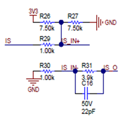
IS_IN+ and IS_IN- are input to the SAC0 and IS_O is the ouput. Same IS_O is the configured as input of the ADC A1. After configuration I see voltage on node IS_IN+ as 1.38V instead of 1.5V.
pin config
// Configure ADC A1 pin
P1SEL0 |= BIT1;
P1SEL1 |= BIT1;
P1SEL0 |= BIT1 + BIT2 + BIT3; // Select P1.1 P1.2 P1.3 OA function
P1SEL1 |= BIT1 + BIT2 + BIT3; // Select P1.1 P1.2 P1.3 OA function
Configuring SAC
SAC0OA = SACEN | OAEN | NMUXEN | NSEL_0 | PMUXEN | PSEL_0;
SAC0PGA = MSEL_2; // non-inverting mode */
Configuring ADC
ADCCTL0 |= ADCSHT_1 | ADCON; // ADCON, S&H=16 ADC clks
ADCCTL1 |= ADCSHP; // ADCCLK = MODOSC; sampling timer
ADCCTL2 &= ~ADCRES; // clear ADCRES in ADCCTL
ADCCTL2 |= ADCRES_2; // 12-bit conversion results
ADCMCTL0 |= ADCINCH_1; // A1 ADC input select; Vref=AVCC
ADCIE |= 0x00; // Enable ADC conv complete interrupt
P1SEL0 |= BIT1 + BIT2 + BIT3; // Select P1.1 P1.2 P1.3 OA function
P1SEL1 |= BIT1 + BIT2 + BIT3; // Select P1.1 P1.2 P1.3 OA function
