This thread has been locked.

If you have a related question, please click the "Ask a related question" button in the top right corner. The newly created question will be automatically linked to this question.

TIDM-DC-DC-BUCK: Lab 1, Open Loop: Plant Frequency Response

Part Number: TIDM-DC-DC-BUCK
Other Parts Discussed in Thread: SFRA

Greetings,

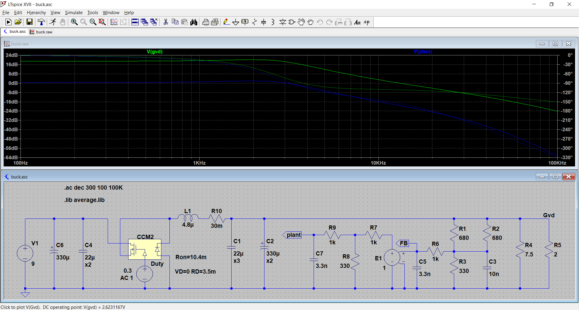
When the Software Frequency Response Analyzer (SFRA) plots the frequency response of the Buck plant (Control-to-Output tranfer function), does it take into account the scaling factors of both the output and input resistive dividers that are used in order to feed the output and input voltage respectively to the ADC pins?

If we did not take any scaling into account, I would expect the plant transfer function of the Buck converter to have a DC gain equal to the input voltage, namely 9V or 19 dB. However, the plot shown has a DC gain just above 0dB.

However, If I scale the plot by multiplying with both the divider ratios, namely [330R, 1K] on the input and [330R, 340R] on the output, then I do get close to the DC gain shown.

Could someone please clarify how the plant function is actually constructed?

Thank you very much.

Kind regards,

Vyron

  • Hi,

    SFRA includes the sensing gain (determined by resistor divider) of the power stage. 

    Please check BUCK_SFRA_INJECT and BUCK_SFRA_COLLECT in SW. It perturbs the duty and collect the frequency response in P.U value not in the actual voltage magnitude.

    Best,

    John

  • Hi John,

    Thank you for your response.

    I expected that SFRA would include the resistive divider sensing gain on the output, which basically scales the measured frequency response by a factor of 330/(330+340), or about 0.5.

    Then the DC magnitude of the frequency response would be 9*0.5=4.5 or 13 dB. This seems to be the magnitude shown in the Open Loop plot on page 28 of the Reference Design. However, the same plot shows low-frequency phase of -180 degrees which I am not sure why is the case.

    Then on page 29 the plant is shown to have the DC gain just above 0 dB, which made me think that there is some extra scaling involved. The scale factor of the resistive divider on the input is 330/(1330), or about 0.25. If I multiply the previous result, 4.5*0.25=1.125 or 1 dB, which seems to match the plot.

    However, I am unclear why the input resistive divider would be taken into account in the frequency response. Is this what is actually happening, or is there something else?

    Unfortunately I do not yet have the actual hardware board so I cant experiment on it. 

    Thanks again.

    Regards,

    Vyron

  • Hi,

    Did you derive the transfer function and check the frequency response from it? 

    Best,

    John

  • Hi John,

    I derived the transfer function and also verified it using Spice simulation, where I have recreated the buck converter circuit I am attaching a screenshot where you can see in green the actual Control-to-output transfer function Gvd(s), and then I have implemented the input and output divider scaling factors as per the EVM and I have obtained a scaled version in blue, which looks like the plant transfer function shown in the Reference Design.

    Thanks,

    Vyron

  • Hi Vyron,

    If you check the mathematical expression of Gvd, it includes input voltage and it impacts the dc gain. As the input voltage is measured by sensing network, it has to consider the sensing gain (resistor divider).

    Best,

    John

  • Hi John,

    OK, thank you for confirming this.

    When it comes to the compensator design though, does the FSRA multiply the compensator transfer function by the inverse of the divider ratio in order to get the correct expression for the loop gain?

    Normally, the loop gain is T(s)=H*Gc(s)*Gvd(s), where:

    H: output sensor gain

    Gc(s): compensator transfer function

    Gvd(s): Converter plant transfer function

    Since Gvd(s) is already scaled by the input divider 330/(1330), or about 0.25, is the compensator actually multiplied by 1/0.25=4 in order to obtain the loop gain?

    Thanks again.

    Regards,

    Vyron

  • Hi Vyron,

    I guess it depends on how you scale the measurement. In this reference design, all the control variables are designed based on P.U value and therefore it is normalized to 1 at the maximum value. Let me know if your model without inverse sensing gain does match with the SFRA plot in the user's guide.

    Best,

    John

  • Hi John,

    I suppose if the whole design is carried out in the SFRA, by adjusting the compensator to shape the loop gain, then the scaling does not matter.

    Only if the compensator is designed separately, i.e. in MATLAB or Spice, then it would need to be appropriately scaled.

    Below I have designed an analog compensator with the same salient features as the digital version in the reference design, apart from the fact that I have divided the KDC factor by 4 to obtain approximately 38000/4=9000. Then, the loop gain seems to be quite similar, especially at the lower frequencies where there is no impact by the delays of the digital implementation.

    In the absence of any poles introduced by the digital loop, as well as the fact that my spice model is only an approximation, I seem to be thus getting similar low frequency gain, but slightly higher crossover and phase margin. 

    Red: plant transfer function Gvd, scaled  by both input and output resistive divider ratios

    Blue: compensator with Kdc=9000, two zeroes at 6 kHz and one pole at 11 kHz, but then multiplied by 4 to get the same as the digital one

    Green: loop gain

  • Hi Vyron,

    Corrects me if I'm wrong. Let me define Gvd in different way. I typically does not include the voltage sensing gain this makes me confuse.

    Gvd is duty to output transfer function and SFRA include voltage sensing gain. Therefore,.

    Gvd = (V(S)/d(S)) * Kgain

    If you need to design a compensator, you need to compensate for (V(S)/d(S)) * Kgain and therefore the inverse of Kgain has to be multiplied. Is this what you get on blue curve?

    Best,

    John