This thread has been locked.

If you have a related question, please click the "Ask a related question" button in the top right corner. The newly created question will be automatically linked to this question.

TIDA-010054: Issues in forward power transfer mode(400V to 48V) in Bidirectional Dual Active Bridge

Part Number: TIDA-010054

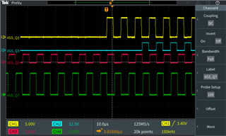
We are trying to transfer power from the primary to secondary side of the DAB converter. Accordingly, all the switches are operated at 50% duty ratio and appropriate deadband has been introduced between the complementary switches of each leg. Also, we have provided phase shift to the gate pulses of the secondary side switches keeping the primary side as the reference. However, the obtained waveforms of inductor current seems to be similar to the ones as shown in Fig. (4.42), page 77 in TI's reference design TIDA-010054. The diagram explains how inductor current should behave during reverse power flow but we are getting similar waveforms during forward power flow. The MOSFETS and the DC-bus capacitors at the secondary side are also getting heated up. To debug this problem, we checked the switching pattern of both the sides of the DAB converter at startup. The switching patterns including the other waveforms are attached herewith for your reference. Please have a look at our results and let us know if we are doing anything incorrectly.

Figure. 1: Switching pattern of both primary and secondary side switches during startup without phase shift

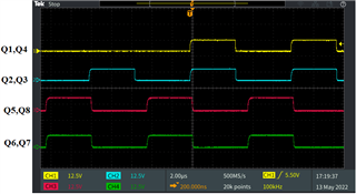
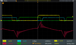
Figure. 2: Primary and Secondary transformer voltages with phase shift and inductor current


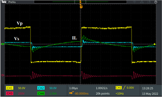
Figure. 3: Gate pulses of Q1 and Q5 with phase shift, Primary transformer voltage and secondary side output capacitor current ripple


  • Hello, 

    1. why in the 1st pic theQ1 and Q5 has a 180 deg phase shift? I thought Q1 and Q2 are the complementary switches, which are in the same HB. 

    2. did you try to limit the inrush current during start-up? starting with very small phase shift

    It will be good that you can attach a schematic or we can have a discussion via a call. 

    Rgds

    Lei

  • Sorry for the inconvenience. Attaching the images here.

    Figure.1: Gate pulses of upper MOSFETs of each leg on primary and secondary side during startup with phase shift. Lower MOSFETs are complementary with appropriate deadband.

    Figure. 2: Gate pulses of upper MOSFETs of each leg on the primary and secondary side during steady state with phase shift. Lower MOSFETs are complementary with appropriate deadband.

    It would be really helpful if we can have a call with you Lei regarding our issues. We can share our schematic during the call.

  • Hello, 

    The gate signal looks okay to me. Do you have any contact to the local FAE of TI? Then let's schedule a call. 

    Rgds

    Lei

  • Yes, we have the contact of Mr. Vikas Chola (vikas.chola@ti.com). He is our local Field Applications Engineer. Shall I contact him to schedule a call or will you do it from your side?

  • Also another question.

    While you guys tested the DAB, what kind of load did you use?

  • yes, pls do it. 

    Rgds

    Lei

  • We use resistive load testing the DAB. 

  • Hi Lei,

    Attaching the present waveforms below.

    The gate pulses are like the images shared in the previous messages.

    Yellow is gate pulse of Q1, Green is gate pulse of Q6, Blue is gate pulse of Q5 and Red is primary side transformer current. Providing 1us phase shift at the moment.

    By considering the intervals in TI's reference design, inductor current is rising during interval 1 during positive half of the transformer voltage as expected but in interval 2 it should steadily rise in the positive direction but it is going negative as shown in the waveform. The input voltage is 10.5V and output voltage is 1.632V. If I consider the slope equation for interval 2, the slope is (Vin - (Vo/n))/L. Considering our turns ratio, n = 5/42 and leakage inductance, L = 34uH, we get negative slope since (Vo/n)>Vin. But ideally in interval 2, (Vo/n)<Vin for positive slope but we are getting the opposite. Can you help us debug this issue?

  • I want to summarize the issue and debugging steps:

    Issues:  

    1. high ringing and spike on secondary tank voltage Vs
    2. wrong inductor current slope

     Suspecting:

    1. high freq ringing caused by the bootstrap gate drive or large Coss of Si FETs
    2. wrong inductor current slope caused by wrong connection of the transformer terminals

     Debugging steps:

    1. try to remove the secondary side FETs gate signals, let the back gate diode to rectify the voltages and see if the ringing still there
    2. try to replace to low Coss Si FETs or use the SiC FETs
    3. try to add DC blocking cap
    4. Pls increase the output cap to more than 150 uF