This thread has been locked.

If you have a related question, please click the "Ask a related question" button in the top right corner. The newly created question will be automatically linked to this question.

TIDA-01102: Ground plane cutouts in reference design

Part Number: TIDA-01102

Hi,

I am designing a board using a printed coil matrix inspired by the TIDA-01102. I am now looking into how to design the ground planes for the board.

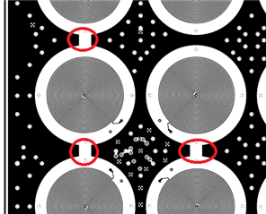
Looking at the TIDA-01102 design, I am struggling to understand why there are cutouts in the copper pours between the coils. Furthermore, why are there cutouts for all the coils in the first and last columns and only two-and-two in the middle columns? From what I know, I would think it would be better without these cutouts. It would be great if someone could explain the reasoning for these, so I may eventually incorporate this in my design.

Best regards,

Håkon Liverud

  • Hello Håkon,

    Thanks for considering to use Texas Instruments.  I presume that the cutouts you are referring to are the areas where the copper was removed indicated by the red circles in the image below.  Unfortunately the employee responsible for that layout does not seem to still be with TI and I cannot find any particular notes with regard to that layout decision.  However, I suspect it might be related to him aligning the coils.  He may have used a line that was originally the same layer as the copper pour, which would create a discontinuity in the copper, then afterwards changed those alignment lines to some non-copper layer and did not update the pour.