This thread has been locked.

If you have a related question, please click the "Ask a related question" button in the top right corner. The newly created question will be automatically linked to this question.

TIDA-020031: Purpose of Schottky Diodes

Part Number: TIDA-020031

Hi,

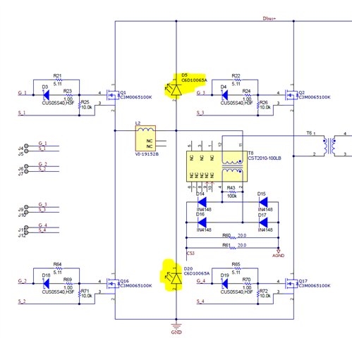
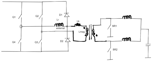
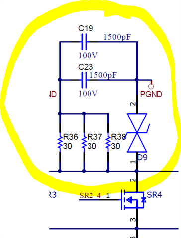
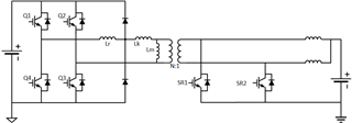
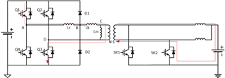
I'm investigating the power stage schematic files of TIDA-020031, which is phase shifted full bridge converter. I'm trying to understand the purpose of schottky diodes mounted as below.

1) Could you please comment on what the purpose is putting such diodes at that node?

2) What is the advantage and disadvantage of putting those diodes?

3) Does D5 prevent charging of Coss of Q17 and discharging of Q2 after turning OFF Q17? 

  • Hi Gokhan,

    Thank you for the question.

    1) Could you please comment on what the purpose is putting such diodes at that node?

    These diodes are clamping diodes, which are used to clamp the secondary voltage, like RCD snubber at the secondary side. For example, if the transformer primary voltage exceeds Dbus+, the diodes will turn on and clamp the primary voltage to Dbus+, that means the secondary voltage is clamped at (Dbus+ / TurnRatio).

    2) What is the advantage and disadvantage of putting those diodes?

    Advantages:

    1. Can select secondary FET with less secondary voltage rating.

    2. Compared to RC or RCD snubber, it doesn't consume the energy on resistor, so it has higher system efficiency.

    Disadvantages:

    1. Extra size and cost.

    2. It only makes sense when external resonant inductor is used. If resonant inductor is integrated as transformer leakage inductance, these diodes cannot clamp the transformer voltage. (Because the voltage drops on leakage inductance)

    3) Does D5 prevent charging of Coss of Q17 and discharging of Q2 after turning OFF Q17? 

    It doesn't. D5 only turns on when its anode exceeds Dbus+ caused by secondary resonance. When turning off Q17, D5 is not turned on before charging and discharging of Coss.

  • Dear Forest,

    Thank you for your clear explanation. It might be out of scope, however, i want to ask followings.

    1) What is the main root of cause of primary voltage spikes? Is it because coss of mosfet and total leakage inductance during mosfet turn-off?

    2) Is there any benefit by clamping diodes during reserve (boost) operation? (When driving as isolated boost topology)

    3) Why is it required when external resonant inductor is used? How doesn't it benefit to spikes caused by transformer leakage inductance?

    4) What about connecting midpoint of clamp diode bridge connecting to pin 2 of transformer?

    5) We observe that clamping diode is starting conduction at the point which isn't expected - it is indicated with red arrow at below-, you can also see connection point in the circuit. Do you have any experience or idea about that issue? I attached figure.

    6) As I understood, the high side diode clamps also the spike caused by Q17 turn-off. High-side diode conducts at power transfer phase and also freewhelling phase? I attached figure.

    Blue: High side diode current, Yellow: Transformer Voltage, Orange: Vds of 1B, Red:Vds of 2B

    7) If diodes aren't mounted, there is no oscillation at transformer voltage during its voltage is rising up. Could you please comment on it?

    Thank you in advance.

  • 1) What is the main root of cause of primary voltage spikes? Is it because coss of mosfet and total leakage inductance during mosfet turn-off?

    That's right. When secondary rectifier mosfet Q6 turns off, its Coss will resonate with leakage inductance Lk, which causes secondary voltage ringing, as shown below. After Lk & Lm is the equivalent ideal transformer, so the voltage ringing will reflect at primary side (The right side of Lk). No voltage spike on the left side of Lk, because the voltage drop is on the Lk.

    2) Is there any benefit by clamping diodes during reserve (boost) operation? (When driving as isolated boost topology)

    We didn't test it before. From my prospective, as long as there is voltage drop on primary leakage inductance, it can benefit the secondary voltage ringing. But when it works in boost mode, the secondary control mode is different, so I cannot evaluate the performance. 

    3) Why is it required when external resonant inductor is used? How doesn't it benefit to spikes caused by transformer leakage inductance?

    As shown below, you can understand in this way. The diode can clamp volatge in Vin, that means it short the Lr, so the actual resonant inductance is Lk, the total resonant energy is reduced from  Lr+Lk to Lk. If the resonant inductance is integrated into transformer, that means Lr=0, in this scenario the diode does not short any inductance. It became meaningless because Q1 and Q3 have internal diodes themselves.

    4) What about connecting midpoint of clamp diode bridge connecting to pin 2 of transformer?

    Good question. It can connect to Pin 2 of transformer. When transformer is between the midpoint of diode and midpoint of lead bridge, it is called Tr-lead topology, while when transformer is between the midpoint of diode and midpoint of lag bridge, it is called Tr-lag topology. Your assumption is Tr-Lead topology, and in the schematic is Tr-lag topology.

    Tr-lag topology has better efficiency because it the diode only turns on one time per switching period, while diodes in the Tr-lead topology turn on two times per switching period. (You can search more documents on Tr-Lead and Tr-lag comparison for details.)  

    5) We observe that clamping diode is starting conduction at the point which isn't expected - it is indicated with red arrow at below-, you can also see connection point in the circuit. Do you have any experience or idea about that issue? I attached figure.

    Did you use Tr-lead topology as I mentioned before? In Tr-lead topology, it indeed turns on two times per switching period.

    6) As I understood, the high side diode clamps also the spike caused by Q17 turn-off. High-side diode conducts at power transfer phase and also freewhelling phase? I attached figure.

    For Tr-Lead topology, it turns on two times per switching period, only one time is used for voltage clamping.

    For Tr-lag topology, it turns on one time per switching period, this time is used for voltage clamping.

    7) If diodes aren't mounted, there is no oscillation at transformer voltage during its voltage is rising up. Could you please comment on it?

    Thank you in advance.

    Did you use external Lr? if not, the primary transformer voltage is clamped by diode of Q1.

    Did you use another clamping circuit at the secondary side? For example, RC snubber, RCD snubber, active clamping. These clamping circuits can suppress the voltage ringing. 

  • Dear Forest,

    Thank you very much for detailed explanation. I really appreciated and satisfied for your answer.

    I need one more step to conclude. 

    We test our designed board and drive switches at open loop configuration. Our board is CD topology and schematic is very close to schematic of TIDA-020031. We drive that Q3 turns OFF during Q1 is ON according to you previous posts schematics. That means our right leg has higher energy for ZVS. Therefore, leading leg is our right leg. The midpoint of clamping diodes are connected to same as schematic of TIDA-020031. However, we have different transformer dot polarity. It isn't same as TIDA-020031. The dot of secondary is at different winding point.

    I inserted diagram as below. 

    Going to my questions after brief explanations.

    Q1) You say that " No voltage spike on the left side of Lk, because the voltage drop is on the Lk." What is the meaning of no voltage drop is on Lk.

    Do you mean this? We turn OFF Q3 when Q1 is ON, so during duty cycle loss mode (charging of external inductance), external inductance is charged before coss charging of SRs. 

    OR

    Do you mean this? There is a reflected spike of SR MOSFETS to primary side of transformer. The Lk is an inductance and inductance can reflect voltage spike through winding itself. Therefore, I think that spike can seen on both pins of Lk. Do you mean that voltage spike on starting winding of Lk doesn't transferred to end of winding.

    By the way, however, this Lk is inside of transformer. So, we cannot probe it. When we probe the primary winding of transformer, we see the spike.

    Q4) As I understood, diode bridge is between leading left (left-leg) and transformer. The QD turns OFF when QA is ON. Therefore, it seems that schematic of TIDA-020031 is Tr-lead topology as you define. Could you please confirm?

    Q5) We think that our case is Tr-lead topology. However, the transformer dot is different. Does it change the topology?

    Q7) We have external shim inductor as I drawed. Yes, we have external clamping circuit as reference design.

    Q8) The last one and new one;

    I see the following waveform when I activated SR MOSFET drives. The blue one is shim inductor current. Yellow is transformer primary voltage. Red is Vds of Q3, Orange isVds of Q4. The current waveform shows that the clamping phase is so much longer. Therefore, I don't see the current increasing at the power transfer interval. The current slopes down during power transfer phase. I imagined that so much spike energy of SRs is reflected to primary and clamping duration phase is increased.

    When I increased load current, clamping interval decreases and I started to see current slope up during power transfer phase, after clamping. If I increase the Vin, the clamping interval also increases and current continue to slope down. Clamping diode has negative side effect at this time. It limits current transfer phase. Could you please comment on it?

    Thank you in advance. 


  • Hi Gokhan,

    Thank you for the feedback. We indeed have a deep dive on this topic. 

    We drive that Q3 turns OFF during Q1 is ON according to you previous posts schematics. That means our right leg has higher energy for ZVS. Therefore, leading leg is our right leg.

    You are right. If you control Q3 and Q1 in this way, the right leg is leading leg, and this topology is Tr-lead topology.

    Q5) We think that our case is Tr-lead topology. However, the transformer dot is different. Does it change the topology?

    SR1 and SR2 are full symmetrical, it doesn't chaange the topology.

    Based on the information, I redraw your topology:

    You say that " No voltage spike on the left side of Lk, because the voltage drop is on the Lk." What is the meaning of no voltage drop is on Lk.

    Maybe I didn't explain clearly before. Tr-lead diode will turn on two times per switching period, one time in freewheeling and one time in power transfer (This time is related to clamping).

    1. One time in freewheeling

    Stage 1: Q1 and Q3 turn on, power transfer in red line. D1 turns off.

    Stage2: Q3 turns off, ILk starts to charge Coss of Q3, Vcd~=Vin cannot vary immediately, so Vc will exceed Vin, cause D1 turns on

    Stage3: Vd is increased to Vin, then Q2 turns on. D1 still turns on.

    Stage4: Q1 turns off, Va will decrease to 0, SR still in freewheeling, so Vab = -Vin. D1 still turns on.

    Stage5: Because Vab = -Vin, ILr drops qiuckly. When it drops to ILk, D1 turns off.

    Therefore, D1 turns on in freewheeling, not related to clamping. 

    2.One time in power transfer

    This time is easier to understand. After duty-cycle loss stage, the secondary voltage will increase, when it arrives at Vin/N, Vc>Vin, cause D1 turns on, until iLr=iLk. 

    Therefore, D1 turns on power transfer stage, this time is related to clamping. 

    Does it meet the waveforms? 

  • Dear Forest,

    Thank you for detailed explanation. We are investigating the issue and answer to you soon.