This thread has been locked.

If you have a related question, please click the "Ask a related question" button in the top right corner. The newly created question will be automatically linked to this question.

TIDA-00663: stack-up (bow and twist problem) and accuracy issues

Part Number: TIDA-00663
Other Parts Discussed in Thread: TDC7200, TPL0202-10

Hi Team,

I have a couple of questions about the design reference TIDA-00663.

1) I am trying to build the TIDA-00663. However, the manufacturer of the PCB noticed that the stack-up could have some problems. In particular, there could be a bow and twist due to the high difference between the thicknesses of layer 4 and layer 8. Is the stack-up (with the order defined by the “Layer” column) in the Gerber file correct ? In this case, how do you suggest to solve this problem?


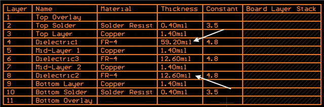
2) Is the entire TIDA-00663 design expected to have an experimentally 1 cm resolution, even considering that the rise time of the pulsed laser "SPL LL90_3" is in the order of 10 ns?


Thank you in advance.

Regards
Giovanni

  • Hi Giovanni,

    Yes the Gerber that you find in the TIDA-00663 page is the one we used to manufacture the boards. We have not faced this problem during the tests of this design. 

     The resolution of this reference design is given by the smallest difference between the two reported distances which is determined by the LSB of the TDC.

    Thanks

    Giovanni

  • Dear Giovanni,
    Thank you for your prompt response.

    Dealing with accuracy, according to your experience and the tests of this design, is this lidar design able to achieve an accuracy in the distance measurement in the range 1cm - 10cm?

    Thank you,
    Regards,
    Giovanni

  • Hi Giovanni, 

    In this reference design, the main focus has been to characterize the differential ToF measurements approach using two TDC7200 devices. The TDC7200 has a blanking time of 12 ns. The TIDA-00663 by using the differential ToF measurements approach allows virtually no blanking time for TDC measurement. However the minimum distance is also a function of optical design so it is important that the field of view of the sensor and the laser overlap to ensure short distance measurements.

    Let me know if you have further questions.

    Thanks

    Giovanni

  • Hi Giovanni,
    Thank you for the reply. The use of differential ToF measurement is clear and is really interesting.

    My question is: can I use this design to measure the distance of a big object (a wall for example at around 5-6 meters away from the lidar) in front of the lidar, with an accuracy of 10-20 centimeters (supposing a good overlap between the field of view of the sensor and the laser and a good reflectivity from the wall)?

    To say it in other words, my question is if this design has been tried as a lidar and can work as lidar for distance measurements or it is only for educational purposes to show the idea of differential ToF measurements?

    I hope my question is clear.

    Best regards,
    Giovanni 

  • Hi Giovanni,

    Yes you can but it has not been tested on our end as this want to be just a reference for customers that want to implement LIDAR by leveraging differential ToF measurements with TDC.

    Let me know if you have any additional questions.

    Thanks

    Giovanni

  • Thank you so much for your prompt response, Giovanni. I really appreciate your help.
    Unfortunately, I received a new feedback from the PCB manufacturer, who is still concerned about the asymmetry (between layer 4 and 8) of the stackup. According to the manufacturer, this would lead to bow and twist (higher than 0.75%), and, consequently, problems in the assembly of SMD components.
    Do you suggest other possibilities to fabricate the PCB without bow and twist? Can I reduce or increase some layers (without performance problems) to make the PCB less asymmetric and avoid bow and twist?

    Moreover, I noticed that the sum of the thicknesses of the layers in the stackup (90.8 mil) in the GERBER file doesn't match the thickness of the PCB (62 mil) in the same GERBER file. Is there something I am missing?


    Thank you for your attention to this matter
    Best Regards,
    Giovanni

  • Hi Giovanni,

    Let me check with the manufacturer that we worked with to build this reference design and I will come back to you by latest the end of the week.

    Thanks

    Giovanni

  • Hi Giovanni,

    You can go ahead and reduce or increase some layers, according to your manufacturers requirements, to make the PCB less asymmetric.

    Thanks

    Giovanni

  • Hi Giovanni,
    Sorry for my late answer and thank you very much for your help. I really appreciated it. I still have some questions about the realization of the PCB.

    1) I followed your advice and made the thicknesses of the dielectric layers symmetric. So, as far as I understand, no impedance control is required for this PCB. Can you confirm it?

    2) I have another doubt. How critical is the R12 (142 kohm) resistor value? The RT0805BRD07142KL part is not available now. Can I use a 143 kohm resistor, instead? I imagine that its value is not critical, since it is only connected to the digital potentiometer. Can you confirm this?

    Thank you again.

    Giovanni

  • Hi Giovanni,

    We have not implemented any impedance control in this design.

    The digital potentiometer determine the two thresholds of the two comparators in the board. The value of these two threshold depends on what you are trying to achieve with your application. Please refer to page 15 of the TPL0202-10 to pick the correct resistor values based on your application requirements. 

    Let me know if there is anything else I can do for you.

    Thanks

    Giovanni