


Hello Everyone
I am building a digital wattmeter intended for measurements on AC power lines. Many designs from Ti Designs and various Application Notes employ a similar frontend where the mains voltage is first scaled down using a voltage divider. The scaled-down voltage signal is then taken as differential and passed through some low pass filter before being fed to a differential-input amplifier or directly to a high-resolution differential-input ADC.

( simplified diagram of the input circuit from SimpleLink™ Wi-Fi® CC3200 Smart Plug Design Guide www.ti.com/.../tidu983.pdf)
After running a simulation of this input circuit, I have found that the ground connection on the Neutral line renders V_SENSE- signal thousands of times smaller than the V_SENSE+ signal, and causes a non-180° phase difference between them. On the contrary, if the connection is removed, V_SENSE+ and V_SENSE- signals are of the same magnitude and 180° relative to each other, creating a perfect differential signal.
1. What is the purpose of this connection from Neutral to the reference ground?
My second confusion is also related to the above-mentioned input section, in a slightly varied form, which appears in many Ti Designs and application notes.
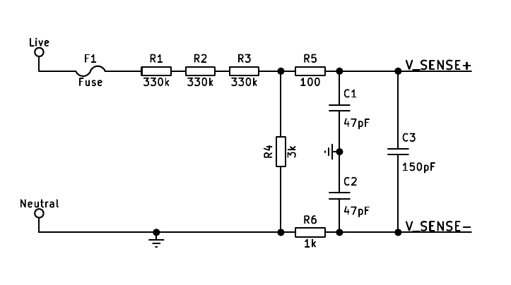
( simplified diagram of the input circuit from Smart Plug with Remote Disconnect and Wi-Fi Connectivity www.ti.com/.../tidu531.pdf)
This is largely the same as the previous configuration. Apart from the differences in components values, the most intriguing difference is in R5, which is 100Ω as opposed to 1kΩ for R6. According to the document, the justification for the smaller value is to make up for the much larger impedance at V_SENSE+. However, simulation results show that the outputs are almost identical to those of the previous configuration. Moreover, the magnitude mismatch and phase angle problems still exist.
The same configuration also appears in
www.ti.com/.../tidu454a.pdf
www.ti.com/.../tidu453.pdf
www.ti.com/.../tidu816.pdf
2. What is the purpose of using a smaller value for R5? Why is it that the previous configuration use the same value for R5 and R6? How do I know when to use which?
Thank you very much :)

