This thread has been locked.

If you have a related question, please click the "Ask a related question" button in the top right corner. The newly created question will be automatically linked to this question.

TIDA-00281: 1Kw controller design

Part Number: TIDA-00281
Other Parts Discussed in Thread: CSD19535KTT, CSD19535

The 1kW bldc controller (TIDA-00281)  Reference Design  provides excellent information for beginners and experts. Which will be more useful for those who eager to know about controllers.

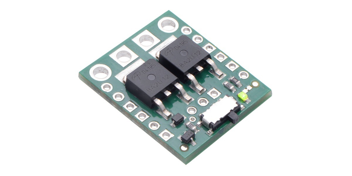
Sir have a doubt , the mosfet that mounded on the PCB (heat sink attached in the PCB). The mosfet's drain is on the backside of fet, so its necessary that individual heat sink should be needed for fets. So in TIDA-00281 design (like the below image) the heat sink is mounded on PCB, is that enough for 1Kw controller. Can you send some reference design of back side of PCB. (The heat sink design)

  • Hi Bud,

    Thanks for asking about this TIDA and sharing your thoughts on the report which I agree with you!

    I am a bit confused because I dont see the heatsink your referring to in the TIDA, when I search in the TIDA there is no heak sink mentioned.
    Are you concerned about the power dissipation on the FET or the driver? if concerned about the driver exceeding juction temp, check out section 2.7 of www.ti.com/.../slua618.pdf

    How much power are you expecting to see across your FET? the Rdson of the FET, peak current and switching frequency will determine the average power dissipated in the FET so you can estimate how much power will need to be absorbed by the heatsink to keep the junction temp of the FET with in limit.

    Thanks,
  • Thank you sir for your response , yes i am concerned about the power dissipation on FET.
    I calculated the losses for your mosfet (CSD19535KTT),
    Major losses, for 48 v 30 amp and for 10 Khz
    Conduction loss = 1.3 W (min)
    switching loss = 1.4 W (min)
    Therefore for 2.7 W, the FET will dissipate 167 degree C(approx).
    Is my above assumption is right ? Else correct me sir.
    My question is , any heat sin is used in the TIDA-00281 or they mounded the heat sink on the pcb itself (like the image i have attached above).
  • Bud,

    There are no discrete heat sinks on the TIDA-00281 board; the MOSFETs have large thermal pads like the devices you show in your photo.  You can find the information for the back side of the board in the "Design files" section of the TIDA-00281 web page. 

    From your calculations, I think you are using the Theta(JA) for the thermal resistance from the Junction to Ambient of 62C/W.  This resistance gets smaller (thermal dissipation improves) as the device is connected to a larger board area.  If you look at the minimum board size around the KTT package (page 8 of the CSD19535 datasheet) there is at least 100 mm2 of area under the device.  The plot below shows how the thermal resistance decreases with increasing board area.  So the layout of the TIDA-00281 will have a lower thermal resistance between MOSFET junctions and the board.  There are several thermal images in the TIDA-00281 design guide that show results for various operating conditions.

  • Thankyou for your reply sir,
    That is for 100mm the theta value is 43C/W. So the power dissipation for 2.7W in the MOSFET will be,
    T = theta*Ploss + 25C
    = 43* 2.7 + 25
    = 139.1 C
    Is it right sir.
    If so then , 139 degree C   is good for a MOSFET(CSD19535) ?

  • You switched from temperature to power in the middle of that equation. 

    Using the values you show above, the junction temperature is around 141 degrees C, which is below the absolute maximum junction temperature for the transistor  (see http://www.ti.com/lit/ds/symlink/csd19535ktt.pdf).

  • Sorry sir, thank you for your response. I wrongly mentioned Watts instead of Celsius. I corrected the above post.
    The fet (CSD19535KTT) has the absolute temperature of 175 degree C, for 100mm area we found that 139 degree C. Is that much heat is good for a FET? . Or my below calculation is wrong
    T = theta*Ploss + 25C
    = 43* 2.7 + 25
    = 141.1 C

  •   43 C/W

     x 2.7 W

    = 116.1 C rise

     + 25.0 C ambient

    = 141.1 C junction temperature

    So if the ambient temperature is 25C, the junction temperature of the FET will be about 141 C, which is well below the absolute maximum rating for this device.