Tool/software: WEBENCH® Design Tools
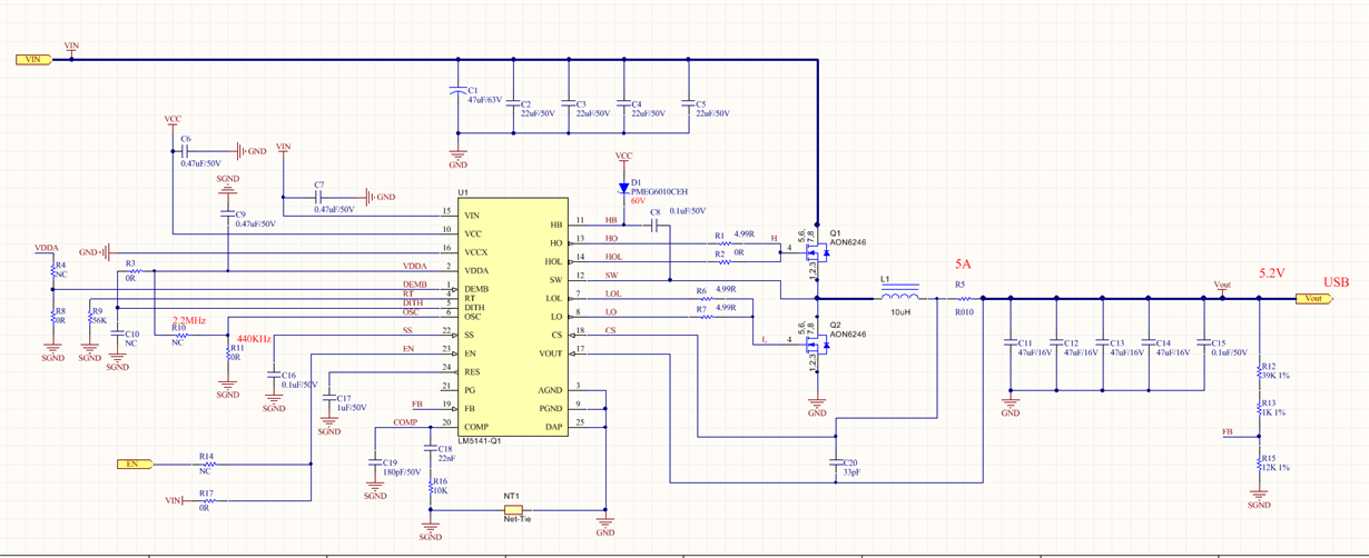
This is my second design LM5141,40V-5.2V DC-DC
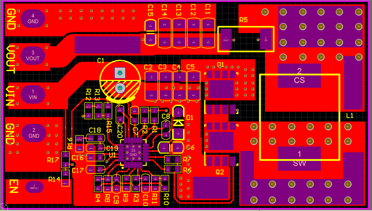
I design the EVM refer to the WENBENCH tool schematic
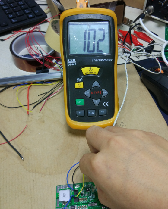
When input is 40V,output is 5.V 3A,IC and MOS are very hot,about 100℃,
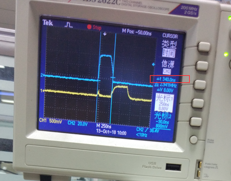
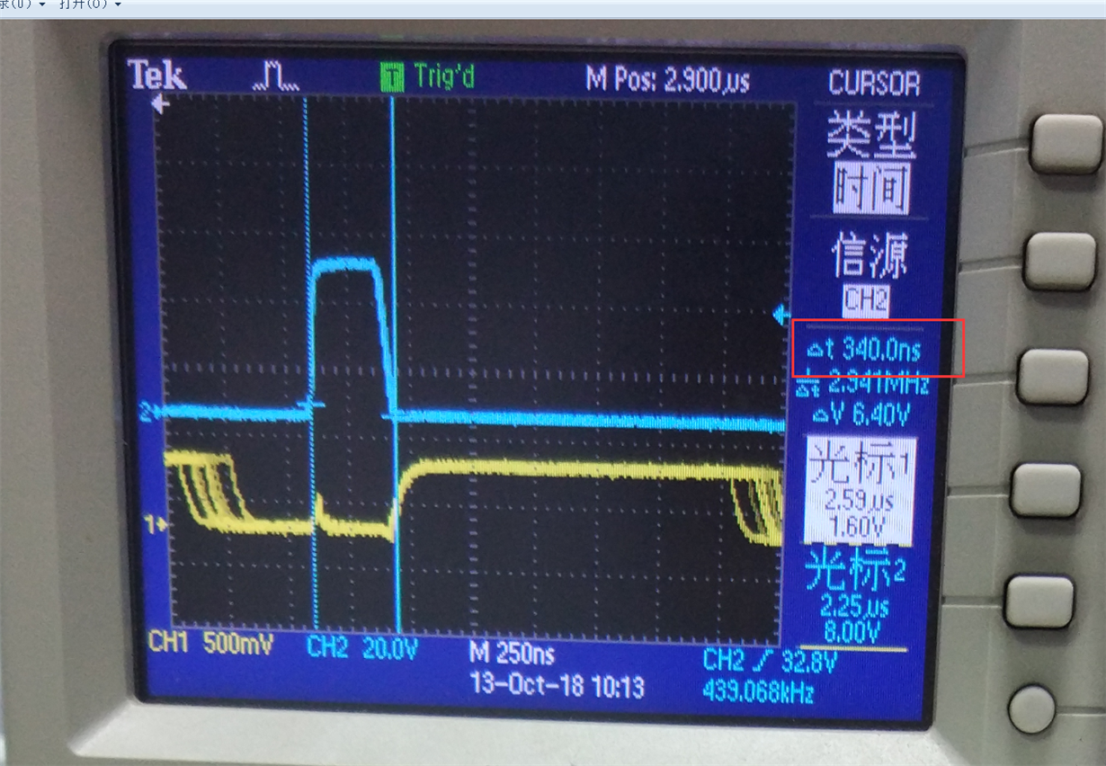
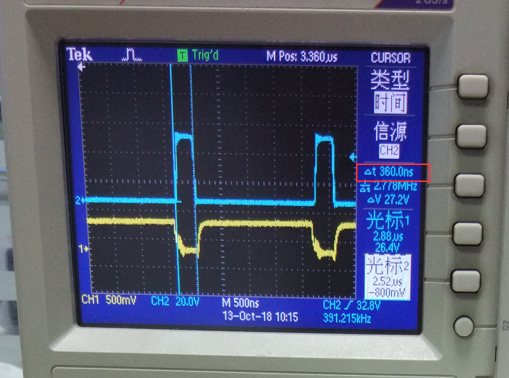
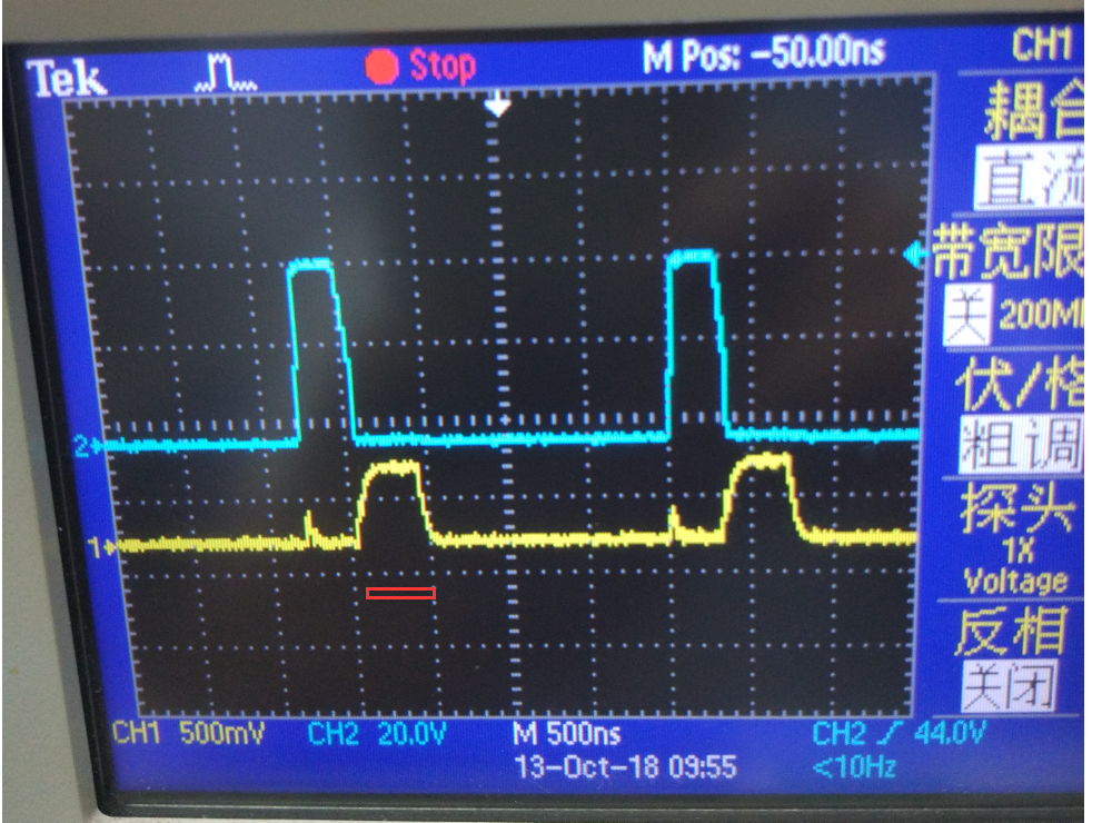
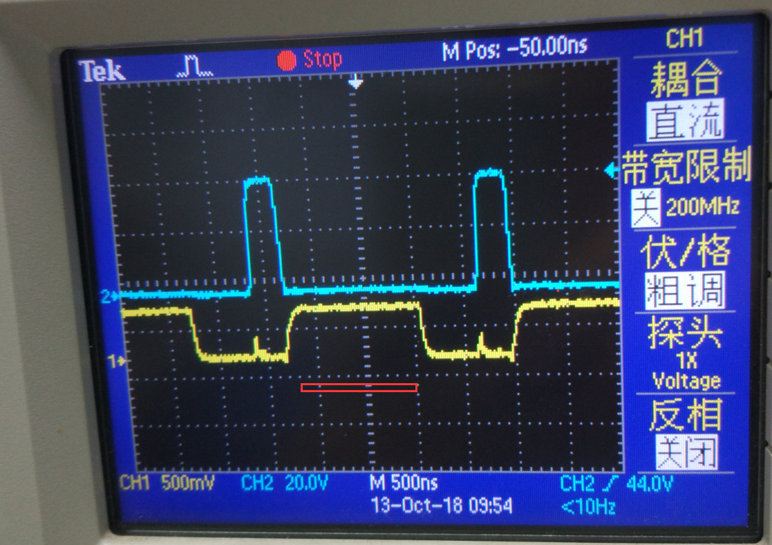
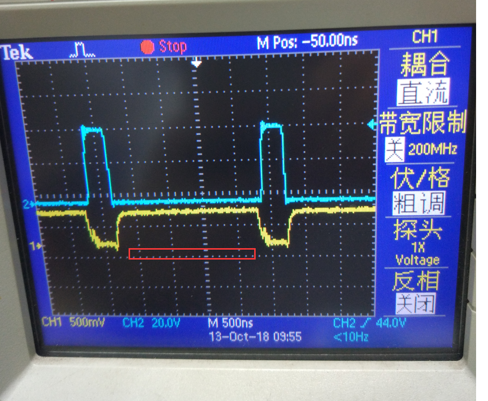
Here are there picture about the high and low MOS driver waves,in different output current。
Blue diagram is high MOS driver
Yellow diagram iS low MOS driver
output is1A
output is 2A
output is3A
See the above there picture,when operate the different output current ,the high MOSFET driver open time almost keep unchanged
Let us see the low MOS diver wave changes in different output current
1A
2A
3A
I am in interrogative ,as usual,when the loading is added,the high driver should gain the duty cycle in the buck circuit,Otherwise this state is not my hope, and why only the low driver duty cycle was added when the output current was added 1A to 3A?
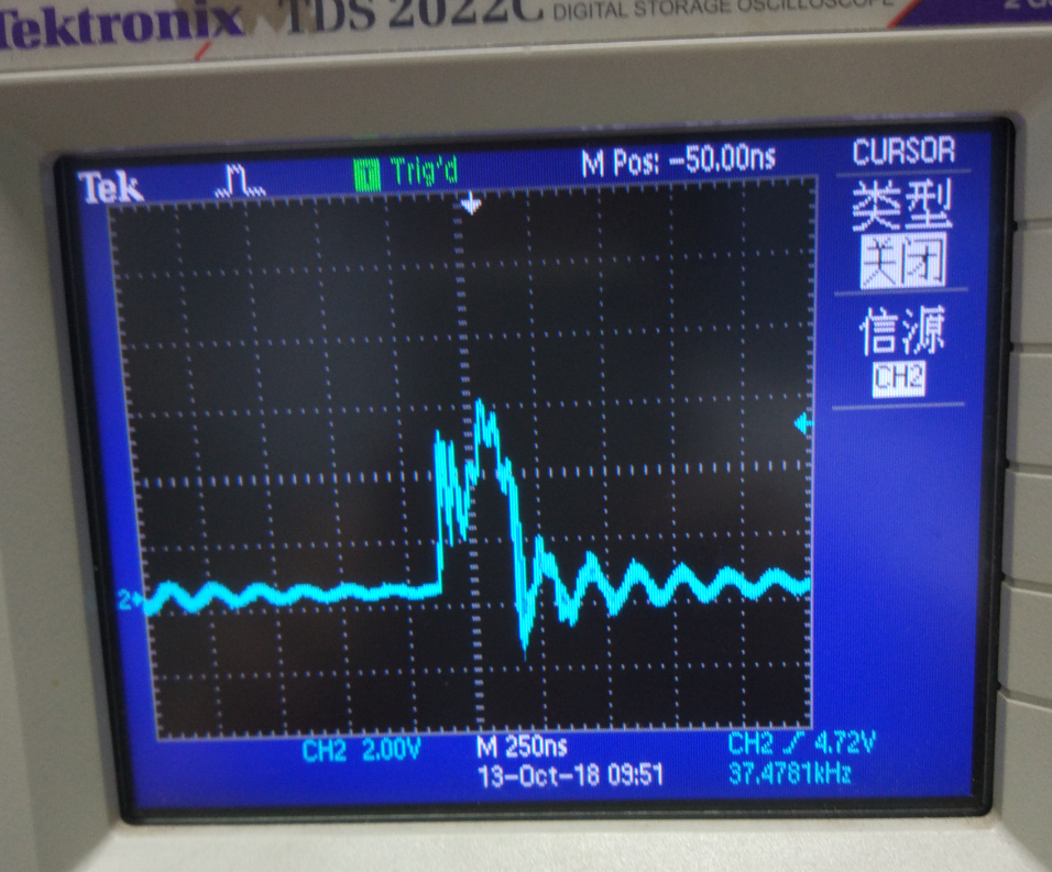
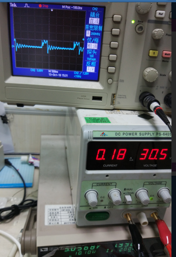
I have test the high MOS Vgs,the wave was very strange
It was seen like not as full work,I gusset if it is the reason why MOSFET was very hot,even the output is only 1A
So my main question is something case the IC and MOSFET hot,I hope someone can help me to solve this problem?
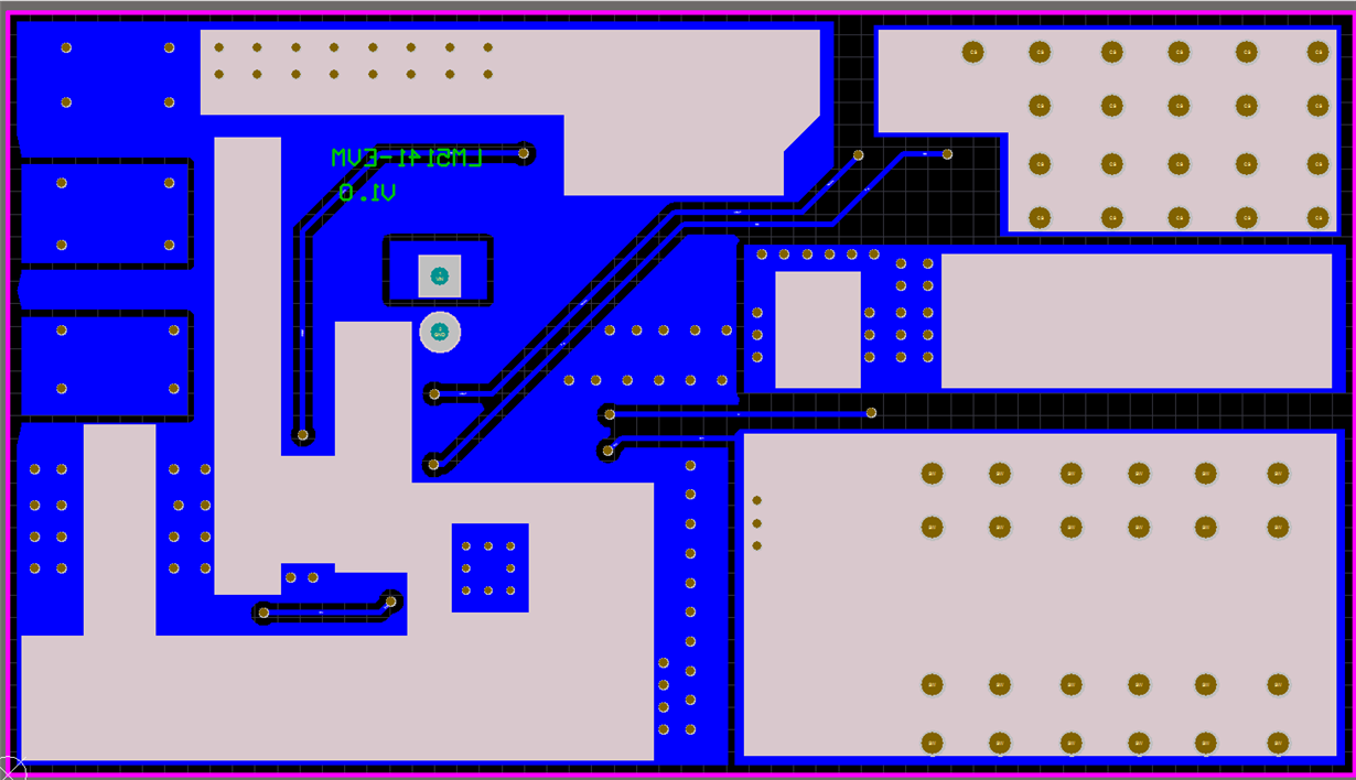
I am sure that IC GND is enough,because the IC is not pover device
I found main reason was that high MOS driver is very weak when the input over 20V
like this pictures:
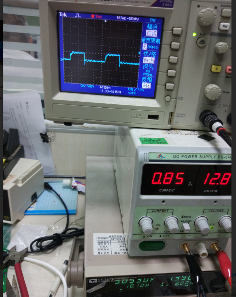
input is 12V,higt MOS Vgs is normal ,IC and MOS can't be hot
input is 30V,higt MOS Vgs wave is Disorderly,IC and MOS are hot
input is 40V,higt MOS Vgs wave is more in trouble
the driver is very weak,so that the MOS be hot when load 。this state I have been understand
But the IC be hot when input is higt voltage,and the driver wave can't serve MOS switch fully,
So what case the IC can't work in high input voltage?


