


Other Parts Discussed in Thread: MSP430F5152,
Tool/software: Code Composer Studio
Hello,
I'm developing MPPT controller using MSP430F5152 based on TIDA-00120 reference design.
I modfied design from the original interleved Buck to 1 channel Buck converter.
To secure proper deadtime, I set the T1CCTL1 and T1CCTL2 value difference to 25, while using reference Timer D initialization routine
with appling MC_3 up down mode. Then I found the PWM deadtime is being changed from almost 50ns to 1.x us without any S/W involvement.
I measure the PWM waveform with both scope and logic anlayzer at breakpoint stopped condition with tmer D free running mode at 256MHz.
Somtime deadtime become almost 50ns and sometimes it become 1.x us. of course, if I make the T1CCTL1 and T1CCTL2 value gap 40,
it was somewhat safe. But it can increase low side body diode conducton loss, I would like to minimize the deadtime.
Why the duty timing is being changed even in breakpoint stop condition in CCS?
the following is the TimerD initialization routne that I applied. And I aso attached simple logic analyzer measured waveform. logic analyzer is just for 24M sample.
So the captured LSB error is about 40nsec. But the showing condtion is almost same when I measured in scope.
CCS ? 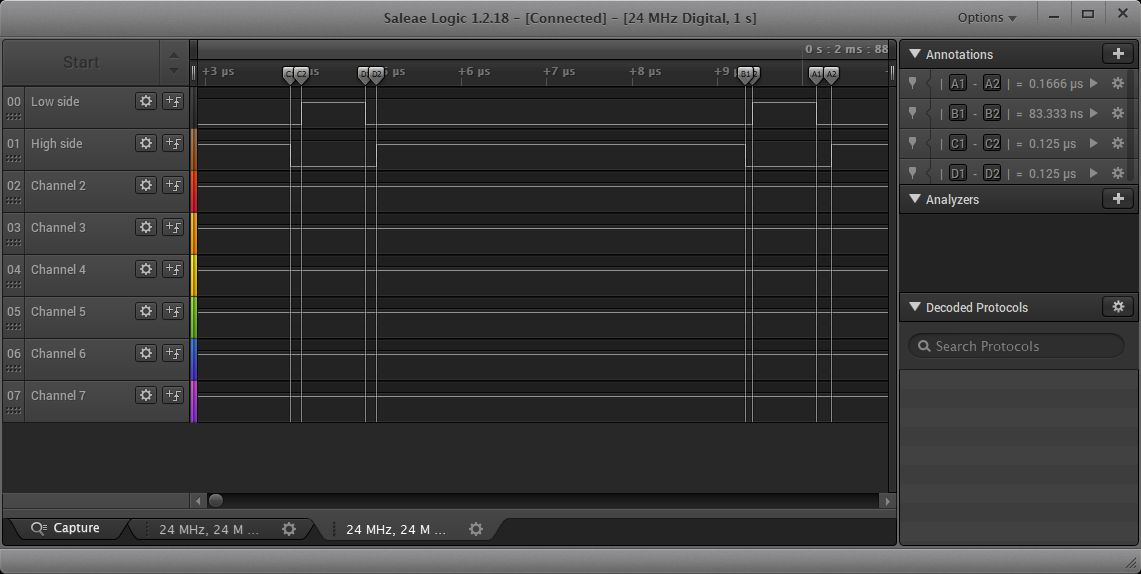
-----------------------------------------------------------------------------------------------------------------------------------
void Init_Timer (void)
{
struct s_TLV_Timer_D_Cal_Data * pTD0CAL; // Structure initialized in tlv.h
unsigned char bTD0CAL_bytes;
// unsigned int i = 20;
// Configure TimerD in Hi-Res Free Running Mode
Get_TLV_Info(TLV_TIMER_D_CAL, 0, &bTD0CAL_bytes, (unsigned int **) &pTD0CAL);
//Get TimerD0 Cal Values (instance 0)
if(bTD0CAL_bytes == 0x0)
{
// No TimerD free running cal data found
while(1); // Loop here
}
// Configure Master Timer Instance - TimerD0, Hi-Res Calibrated Mode
TD1CTL0 = TDSSEL_2; // TDCLK = SMCLK = 25MHz = Hi-Res input clk select
TD1HCTL1 = pTD0CAL->TDH0CTL1_256; // Read the 256Mhz TimerD TLV Data
TD1CTL1 |= TDCLKM_1; // Select Hi-res local clock
TD0HCTL0 = TDHEN + TDHM_1; // CALEN=0 => free running mode; enable Hi-res mode
TD1HCTL0 = TDHEN + TDHM_1; // CALEN=0 => free running mode; enable Hi-res mode // TDHM_0 => 256Mhz, TDHM_1 = > 256Mhz
// Here Timer D is configured to run at 256Mhz
TD1CCR0 = 700; // 256M up down /700 = 182.8Khz is the operating frequency of the buck stage
TD1CCTL0 |= CCIE; // interrupt is enabled to adjust phase
TD1CCR1 = Duty- Deadtime ; // Low side PW_L2? High side PW_H1 *****
TD1CCTL1 |= OUTMOD_2; // TD0CCR1, Reset/Set (outmode2-> toggle &reset ?)
TD1CCR2 = Duty ; // Duty-25 is done to provide Dead Band. Highside PW_H2. PW_L1
TD1CCTL2 |= OUTMOD_6; // TD0CCR2, Set/reset
TEC1XCTL2 |= TECAXCLREN; // Enable synchronized clear by enabling Aux clear of slave timer
TD1CTL0 |= MC_3 + TDCLR; // up&down-mode, clear TDR, Start timer -UP&down -Modified by YSK
}
#pragma vector=TIMER1_D0_VECTOR
__interrupt void TIMER1_D0_ISR(void)
{
TD1CCTL0 &= ~CCIE;
Phase_Shifting_Done = 1;
}
#pragma vector=TIMER1_D1_VECTOR
__interrupt void TIMER1_D1_ISR(void)
{
switch(__even_in_range(TD1IV,30))
{
case 0: break; // No interrupt
case 2: break; // CCR1 not used
case 4: break; // CCR2 not used
case 6: break; // reserved
case 8: break; // reserved
case 10: break; // reserved
case 12: break; // reserved
case 14: break;
case 16: break;
case 18: // Clock fail low
while(1); // Input ref clock freq too low; trap here
case 20: // Clock fail high
while(1); // Input ref clock freq too high; trap here
case 22: // Hi-res freq locked
// Hi-Res freq locked; now configure ports to output PWMs at TD0/TD1
P1SEL |= BIT7; // P1.6/TD0.0, P1.7,TD0.1, options select
P1
DIR |= BIT6 + BIT7; // Output direction
P2SEL |= BIT0 + BIT2 + BIT3; // P2.0/TD0.2, P2.1/TD1.0, P2.2/TD1.1, P2.3/TD1.2, options select
P2DIR |= BIT0 + BIT2 + BIT3; // Output direction
__bic_SR_register_on_exit(LPM0_bits + GIE); // Exit LPM0 on return to main
break;
case 24: break; // Hi-res freq unlocked
case 26: break; // reserved
case 28: break; // reserved
case 30: break; // reserved
default: break;
}
}
TD1CCTL1 = OUTMOD_2; // output mode
TD1CCTL2 = OUTMOD_6; // output mod
----------------------------------------------------------------------------------------------------------------------------------------
I would appreciate your advice on it !
YS Kim

