This thread has been locked.

If you have a related question, please click the "Ask a related question" button in the top right corner. The newly created question will be automatically linked to this question.

TIDA-01605: Output GATE pulses are not as expected

Part Number: TIDA-01605
Other Parts Discussed in Thread: LAUNCHXL-F28379D, , CSD19536KCS

Hello Team TI,

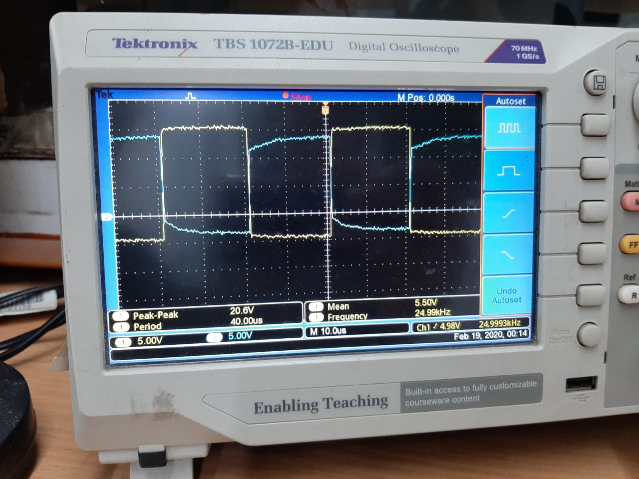
I have tried TIDA-01605 circuit as given in updated schematic. When I gave 5V input supply and Vg1 and Vg2 (pulses from the Launchxl-F28379D) with 25kHz frequency (and with 100kHz frequency too), I found following results. In these results yellow pulses are for switch 1 and blue pulses are for second switch. Here blue one is not 20V_peak_to_peak (+16V and -4V). However, blue one is getting slope also. WHat could be the possible explanation for this? And, how to rectify this problem?

First figure is with 25kHz switching frequency and second figure is with 25kHz switching frequency and 0.22usec dead time.

  • Hi Utsav,

    Did you apply any load to the high side and low side drivers? Because the output waveform will not be pure square due to the influence of parastics. How the test diagram looks like? I recommend to measure the high side and low side PWMs separately with inductive load and MOSFET as shown in the configuration of an inductive switching test.

  • Hello Xun,

    Thanks for your prompt reply. I did not applied any load. I am generating pulses in open end conditions.

  • Hello Xun,

    You can see in the results that peak to peak voltage here is 20.6V which should not be more than 20V in any case. We are providing 15V and -4V supply, then output should be around 19V. What would be the possible solution to fix this problem? Is it possible to solve this problem if I increase the gate resistance (Ron) and provide a zener diode for -4V?

    Thank You

    /

  • Hi Utsav,

    Are the probes and oscilloscope settings are exactly same for Ch1 and Ch2?  Can you switching the probes for measuring the top gate and bottom gate and check if it is still the same driver has 20.6V peak to peak?

    Regards,

    Gangyao

  • Hello Mr. Gangyao Wang,

    Thank for your reply. Yes,  I checked it. In this case channel 1 (yellow one) will exhibit the same performance as the blue one in previous case. So, I guess there is an issue in hardware side. Moreover, output of G1 and S1 shouldn't be more than 20V. For high frequencies such that 200kHz, It is under 20V because magnitude of flat portion reduces and spikes are of 1V only. However in lesser frequencies such that 100kHz it is more than 20V due to spikes. Is there any solution for the spikes (like zener diode or capacitors)?

    Thank You.

  • Hi Utsav,

    Thanks for checking, could you also check the power supply voltage with multimeter or probes?  I mean voltages across C1, C8, C9 and C15. Please also check if input voltage (across C2, C10) is 5V. The auxiliary power supply is open loop with fixed ratio 1:3.9.

    And what is connected to G1, S1, G2, S2? if these are floating, where D2 is connected to?

    Regards,

    Gangyao  

  • Hello Mr. Wang,

    Voltage across the input and output capacitors of power supplies are as follows,

    C2=5.16V; C10=5.16V

    C1=12.36V; C8=6.8V

    C9=15.24V; C15=3.77V

    I have connected two switches for boost configuration (replaces one diode with a switch and it's not a half bridge configuration). Drain of both switches are connected with each other and source are floating points. G1 and G2 are connected with two different CSD19536KCS MOSFETs and S1 and S2 are floating point.