This thread has been locked.

If you have a related question, please click the "Ask a related question" button in the top right corner. The newly created question will be automatically linked to this question.

TIDA-00774: DRV8323S Current Sense Amplifier signal connection questions

Part Number: TIDA-00774
Other Parts Discussed in Thread: DRV8323

Hi,

I am interested in the portion of the TIDA-00774 which relates to the single Low-Side Current Sense Amplifier.  I understand that in this this Reference Design, R17 and R18 are not populated and the CSA is disabled.

However, I have a few questions which I hope you can answer.

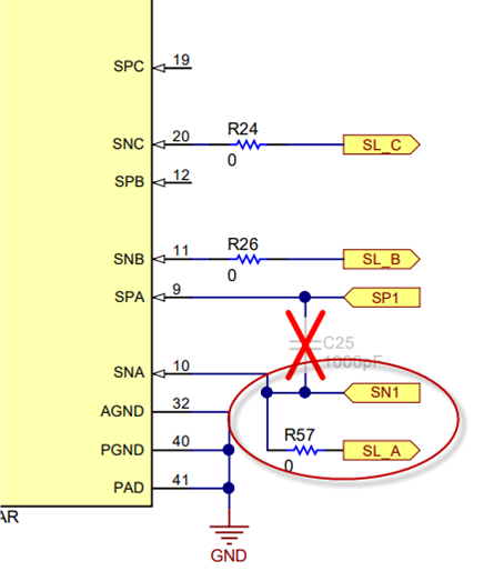
Question #1 - The Current Sense Amplifiers for Phases B and C are not used.  The datasheet indicates "If any of the three current sense amplifiers are not being used, they can be tied off by shorting the

SNx pin to the SPx pin and leaving the SOx pin unconnected".  Why are the SPC-SNC and SPB-SNB not shorted together?  Is there a technical advantage to leaving these inputs open?

Question #2 - The SNA input is tied to both SL_A and SN1.  SN1 is connected to the Battery Ground side of the Sense Resistor while SNx is shown in the Datasheet as connecting to the MOSFET-side of the Sense Resistor.  Is there a reason for connecting SNA to SL_A and SN1 instead of connecting SPA to SL_A and SP1?


Thanks,

Tom

  • Tom,

    Let me look into this and get back to you this week.

    Regards,

    -Adam

  • Hi Adam,

    I compared the layout against the configuration in TIDA-00774_Firmware_V1.0.  I think I understand a bit more now.

    Regarding Question #1, in the DRV8323 configuration, the CSA_FET bit is set to 1 which enables the MOSFET VDS Sense Mode.  In the description of this mode, the reference document states that:  "During this mode of operation, the SPx pins should stay disconnected."  So, now i understand why the SPx and SNx pins are not shorted externally.

    Regarding Question #2, I think the MOSFET VDS Sense Mode explains why the SL_A net is tie to the SNA input since the sense resistor has been disconnected in favor of the MOSFET VDS Sensing.

    If the TIDA-00774 Reference Design was using the single low side sense resistor, then I assume that the SPA input should be connected to the SL_A and SP1 nets.  Does that sound correct?

    Also, think the firmware also disables Gate Drive Faults (SPI_Write(0x02, 0x0100);).  Do you know why Gate Drive Faults are disabled for this reference design?

    Thanks,

    Tom

  • Tom,

    Sorry for the delay here, I had to get in touch with the designer.

    Here are their comments:

    If the TIDA-00774 Reference Design was using the single low side sense resistor, then I assume that the SPA input should be connected to the SL_A and SP1 nets.  Does that sound correct? – Yes this is correct. The SPA pin will be connected to SP1 & the SNA pin will be connected to SN1 , and then mount R17 and R18 to enable single low side current sense

    Also, think the firmware also disables Gate Drive Faults (SPI_Write(0x02, 0x0100);).  Do you know why Gate Drive Faults are disabled for this reference design? – The user can activate the GD fault. I think, I kept the  GD fault disabled to eliminate any initial faults if a wrong IDRIVE/TDRIVE setting is used. User can tune the IDRIVE/TDRIVE setting base on their application and then enable the GD fault.

    Regards,

    -Adam