Hello,
We are manufacting some TIDA-020004 boards to evaluate.
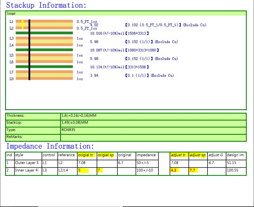
Our PCB manufacturer needed to slightly change the stackup from what TI recommended in the reference design.
They suggested modifying the trace widths and spacing to make sure the impedance is correct, as in attached image
I believe this is okay, but is there any reason this combination of stackup and trace width/spacing would be an issue?
Regards
Brant