This thread has been locked.

If you have a related question, please click the "Ask a related question" button in the top right corner. The newly created question will be automatically linked to this question.

TIDA-060030: RC values for low-pass filtering

Part Number: TIDA-060030
Other Parts Discussed in Thread: MSP430F5529, DRV8343-Q1, TMS320F28035

Hi,

I have a question on RC values for TMS320F28035 MCU low-pass filtering used in TIDA-060030 board. The current sensing pins, ISEN_A, ISEN_B, ISEN_C use R=56 ohms and C=2200pF, which leads to very fast time constant, about 120 ns. I check the datasheet of TMS320F28035, ADC conversion time is 217 ns in Table 3-1. Assuming 1% error, 5 times RC equals to 600 ns, which is larger than the ADC conversion time of 217 ns. I am wondering whether the C of 2200 pF is too large in this EVM board design. Please advise.

Another question is which frequency the TIDA-060030 design try to filter? For 45KHz PWM, it seems to me that above 45KHz frequency should be filtered. If this is the case, RC should be about 1/(5*f_sw) = 4.5 us. From this perspective, both R and C should be larger. My understanding is that C value should be larger than C_SAMPLE inside the MCU so that C_SAMPLE can be fully charged. Does the MCU has a maximum RC value limit? If yes, what is it?

Thus, I am confused. I will appreciate your insight in RC filter design for ADC.

Thanks,

John

  • Hi John,

    Thank you for posting to the MD forum!

    The values used for the RC filter (R = 56 ohms and C = 2200pF) were used from the DRV8343-Q1 EVM schematic. In the TIDA-060030 reference design, the SOx feedback signals were routed back to the MCU but we didn't develop firmware to test the current feedback in the reference design as it was already used in the DRV8343-Q1 EVM with the MSP430F5529 MCU. 

    Let me check with my team to discuss how these filtering values affects ADC conversion time. I will get back to you before the end of the week.

    This reference design uses a PWM frequency of 20kHz. The frequency that is filtered should be about 1.3MHz to filter any high frequency noise from the SOx signals. 

  • Hi John,

    To provide some background information, the TIDA-060030 reference design is designed for driving solenoid loads. The external MCU (TMS320F28035) is used because it has a small package, smaller number of pins used, and the C2000 provided the input control signals to the DRV8343-Q1 using the ePWM module. Although current feedback is routed back to the ADC pins of the TMS320F28035, firmware was never developed in this design for current feedback because it is not needed for its intended application. 

    In regards to determining how the filtering values relates to ADC conversion time, that is beyond the scope of our business unit since we're not the experts on filtering and ADC conversion times. I can go ahead and forward this question to the C2000 team to provide a more insightful answer.


  • Hi Aaron,

    Thank you very much for your quick reply. I will appreciate if you could forward this questions to the C2000 team. RC filtering for a MCU is a difficult topic.

    Thanks and have a nice weekend,

    John

  • Hi John,

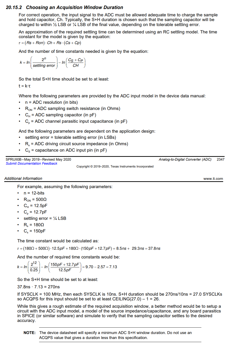
    As far as determining the settling time, please use the following guide from the F2838x TRM to determine the settling time (using the F28035 values for the input model).  

    In general, the RC directly on the ADC pin is not set primarily for filtering purposes. The primary use of the C is to stabilize the ADC input due to the inrush current from the sampling switch closing, preventing the driving op-amp from slewing.  Usually 20 x Ch is sufficient for this purpose.  The primary use of the R is to keep the driving op-amp stable, and usually 20-80 ohms is sufficient. 

    If some light LP filtering is desired, these RC values can be increased a little bit to filter out high frequency noise.  If a true anti-aliasing filter is desired, this needs to be built into a stage of the signal path other than the ADC drive stage as setting the RC large enough for anti-aliasing will result in settling much slower than needed.  

    Alternately, if no op-amp is to be used, the 'charge sharing' method of input design can be used, in which case the C is set to a very large value (resulting in a very short S+H time but a limitation on sample rate).

    For a more exhaustive treatment of the topic, see https://training.ti.com/ti-precision-labs-adcs-introduction-sar-adc-front-end-component-selection and subsequent videos.  


  • Hi Devin,

    Thank you so much for providing such insightful explanations and informative links. I read the materials and watched the videos. They are great.

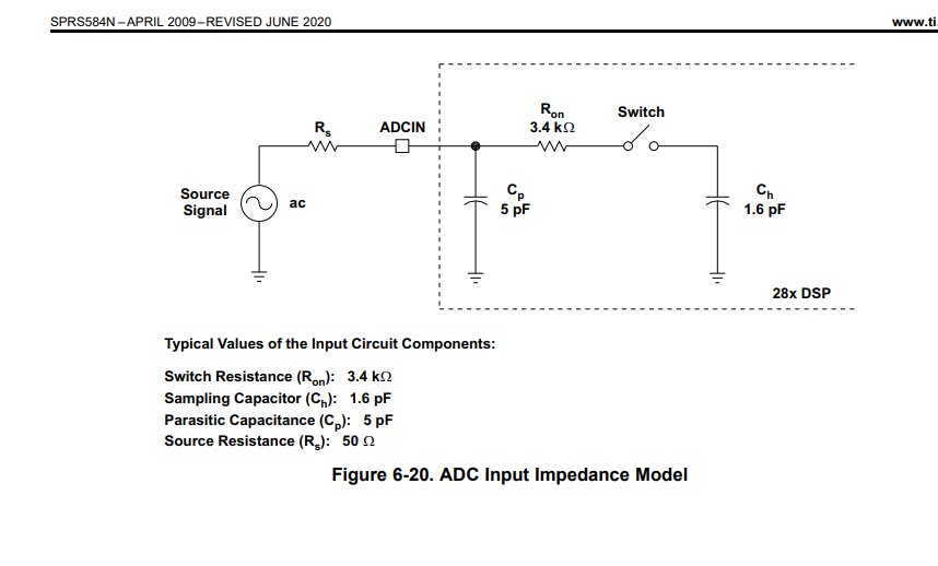
    Regarding the C_filter and R_filter selection, I am still wondering why C_filter in DRV8343-Q1 EVM selected was so large. Based on your recommendation as well as the calculation method described in the video, C_filter should be 20x of C_hold. Fig. 6-20 of the TMS320 datasheet you attached shows C_h = 1.6 pF and C_p = 5 pF. Thus, C_filter = 20 * (1.6 + 5) = 132 pF. The maximum C_filter = 30 * (1.6 + 5) = 198 pF. However, C_filter of 2200 pF was selected in DRV8343-Q1 EVM as well as other TIDA reference designs. Could you please advise whether it was an error or there were other considerations? Would it be better to change the C_filter from 2200 pF to 110 pF? Are there any disadvantages with the small C_filter of 110 pF?

    Thanks again for your help,

    John

  • Hi John,

    I can only speak from the perspective of the ADC.  

    From an ADC settling speed perspective, there isn't any advantage of using 2200pF vs the optimal smaller value of say ~220pF.  The smaller value will give faster settling time.

    However, the external RC does still provide some LP filtering, so 56pF + 2200pF = 1.3MHz cutoff vs. 56pF + 220pF = 13MHz.  If there isn't a dedicated filter stage immediately preceding this drive stage, then this may be helpful, especially if the increased ADC conversion time isn't too detrimental to the system. 

    You may have to play around with this experimentally to determine if performance is being limited by input settling or by noise or by ADC latency.  In your own design, if max performance is the only concern, you can get great filtering and fast settling to the full 12 bit resolution by using an op-amp filter stage (or stages) then an op-amp drive stage, but obviously this will require additional BOM cost and PCB area.    


  • Hi Devin,

    Thank you so much for your time and expertise in answering my question. Your responses are very insightful.

    Thanks and best regards,

    John