This thread has been locked.

If you have a related question, please click the "Ask a related question" button in the top right corner. The newly created question will be automatically linked to this question.

PMP8740: PMP8740 reference design

Part Number: PMP8740

Hi TI Expert , 

I just build a Phase Shift FB converter prototype by exactly copy that PSFB circuit and gerber from PMP8740. 

( but I did not use the micron control , just using  manual analog control of the CC/CV ).

It is my 1st time to study PSFB . I use a 400V DC power to power this poto type ,

it work and I just operate to charge a 100AH 36V Lead Acid battery at no large than 6A.

I won't add more charge current because I'm not sure that FB waveform is healthy or not. 

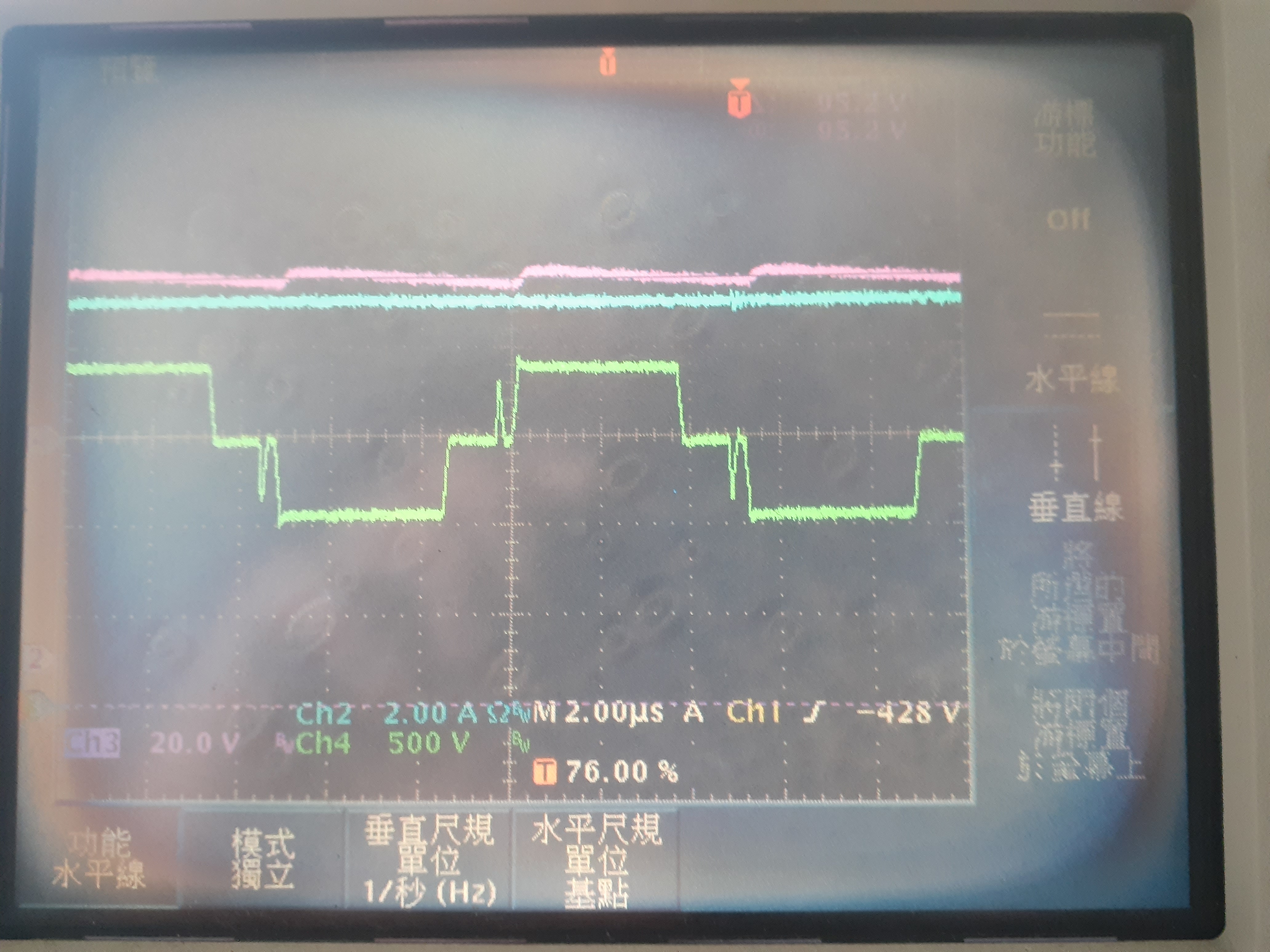
FB waveform in yellow color is attached by differential probing between FB MOSFET Q15 & Q16 Drain electrode 

and I also add OUT E and OUT F waveform ( one in blue , one in pink )  to compare the timing. 

I notice whenever  a High to low on OUT E or OUT F , there always has a spike-like waveform on FB 

My question is if this spike-like normal ? why it appear ? seems it trigger the OUT E or OUT F H to L, 

or vice versa .  I try to read some PSFB paper , just can't explain that on my own . Thank you for help!

Best regards,

Norman

  • Hi Norman,

    please have a look at Test Report page 10, you see almost the same FB waveform there;
    at our prototype it seems to be more ringing, but load current here is 50A, so much more
    energy in the system and in the leakage inductance (by I^2).

    Check thermal behavior by IR camera or similar, check effcy 95%..96%; then I would increase
    current step by step, furthermore please put a probe across burden resistor R34/16.2 Ohms
    to monitor the current.

    I would expect that you changed secondary side; our design is desired for 24Vout, yours for 36Vout;
    means windings ratio, synchronous rectifiers, output caps etc. have been modified.
    To charge 36V lead acid expect Vout 37.8V up to 43.2V, depends on battery condition and chemistry,
    i.e. AGM needs slightly bigger voltage, especially at lower temperature.
    (the uProc usually is taking care of this control & monitoring, you could implement chemistries there,
    means various CC/CV charging curves).

    But to answer your question, on a very first glance your waveform doesn't scare me.

    Best regards, Bernd

  • Thank you Bernd , 

    Sure !  let my increase the current by monitor on what you guided ~ 

     +++ Yes ! nothing works without power +++

  • Hi Bernd ,

    I actually build 48V battery charger by using a 28T:5T PSFB transformer and Lout for L3=22uH ( I calculate that from TI Webench).

    for bring it up step by step  , I now use Fast diode for each output winding in temporary  ( i.e., no sync. rectify mos at present ) .

    I'm interested on the purpose of R98 , D13 , C64, C74, C75, C76  this block. I measure waveform ( pink color ) across R98

    ( Vout as the reference , ~ 100V  drop across R98,  ~ 10W loss , ) , load condition now is Vout ~ 50V and 8A ( that blue line ) .

    heading 60V / 20A for future target which need sync. rectify then.

    I can't figure out the purpose against this 10W loss . Thank you in advance for your comment.

    Best regards

    Norman

  • Hello Norman,

    the purpose of all those element is a RCD snubber circuitry;
    depending on the quality of your transformer you got a certain coupling <1;
    this results in leakage inductance.
    (take your transformer, make a short across primary side, measure the inductance on secondary side;
     that's your leakage inductance at secondary side; should be less than 1% of secondary inductance,
     means coupling >99%; a coupling of 99.5% is feasible for such a large xfmr)

    The leakage inductance stores energy, causes ringing by switching the transformer;
    this ringing, the voltage spike needs to be clamped by RCD snubber circuitry to protect rectifier.
    Have a look at test report page 10, the waveform of secondary rectifiers - you could see the clamping of the spike
    (blue waveform). The voltage by time area that you are clamping are the losses at the resistor.

    10W at your resistor could have two reasons:
    either transformer is poor, so leakage inductance is large, coupling is low - a lot of leakage energy burned at resistor
    or you are clamping too hard, clamping level is very low.

    Check quality of your transformer and use rectifiers with reasonable voltage margin;
    this margin allows you some overshoot, so less energy at the clamping circuit.

    Best regards, Bernd