A related question is a question created from another question. When the related question is created, it will be automatically linked to the original question.
If you have a related question, please click the "Ask a related question" button in the top right corner. The newly created question will be automatically linked to this question.
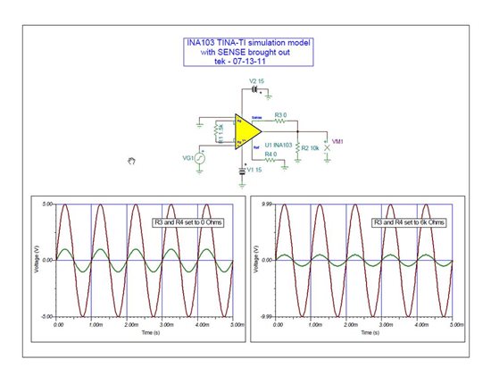
footprint of ina103 has 10 node instead of 16 (dip) in tina-ti
The macromodel that TI has created for the INA103 has only ten (external) nodes - the model assumes that -Gain Sense is connected to -RG, and +Gain Sense is connected to +RG. It further assumes that Sense is connected to the Output. There is no provision for modeling the Offset Null pins, nor are the Gain Drive pins brought out. For most applications, this model does what most people would want for this device - as those default connections are how it is usually hooked up. Does your application require something more, or are you only concerned that the numbers of pins don't match?
I'm sorry, I can't see the pictures, but the model is different from the actual package. Are you trying to lay out the PCB in TINA Industrial? You may have to ask DesignSoft for their suggestion on how to deal with this. There may be a way to create a new schematic symbol for TINA that would allow you to use their PCB package, but I'm afraid we can't be much help there - TINA-TI doesn't have the PCB capabilities and we don't use them here ;-)
I think some people may want to add circuits between the Sense and Output pins, and since you have wired the Sense pin out, how about leave it open? and let the users make the connection as they want?
here is my question:
If I want to break the connection between the Sense and the Output, how to modify the model?
We need to do a little work on this to be able to put it into the TINA-TI library, but we'll do this as soon as possible and will make it available as an update. Until then, you can either just copy the symbol out of the schematic and place it in your own, or use the .TSM file using Insert->Macro menu command.
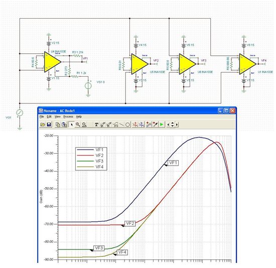
What you've plotted is the AC response of the circuit, not the CMR. Those curves show you 20*log(VFx) plotted against frequency, where VFx is the output voltage from the amplifier.
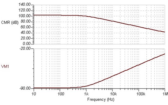
Using the test circuit that I posted the other day, with the amplifier configured for a gain of 5, and 1V in, I get 5Vp out. If I then tie the two inputs together, what I'm interested in is how much signal comes out - that's VM1 in that circuit. But the CMR is the ratio of the output for a regular differential signal to the common mode signal output. So, to get the plots to look like you expect, use the post-processor and set up a new waveform with the equation 5/VM1, and plot that on a Linear-dB scale. Here's what I get: