Other Parts Discussed in Thread: UCC28950
Hi ,
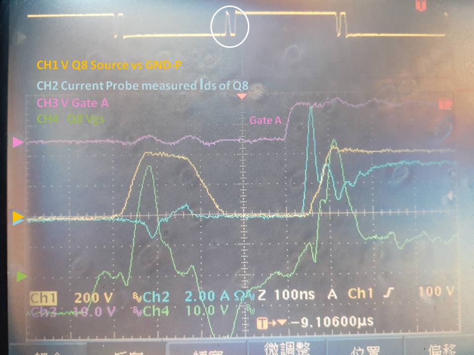
I had some finding , previously that I called a spike on T4 primary ( I labeled it as an abnormal rise then fall to 0V in Fig-B ) may not leakage ringing.
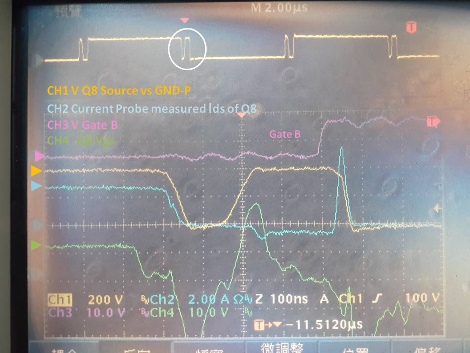
Fig-A, B, C, D as attached . from Fig C and Fig-D , I thought it is because T2 gate drive Vpin8-pin7 , gate B H to L make T2
had 1st trial to turn on Q8 a little, but soon undershoot pull Q8 off at once , followed by gate A L to H that really turn Q8 on . my waveform of T2 8-7 may or may not TI original design looks.
I change the R78 , or R71 and R76 for 2-4 times higher , resonant waveform ( Fig-D green ) always stay the same.
Furthermore , DC level of T2 Vpin1-pin4 waveform at Fig -C is weird to me , should C43 remove the AC content ? I use the same component value and exact T2 from TI BOM. BTW, T2 Vpin6-pin5 is
more , not like T2 pin8-pin7 huge overshoot and undershoot.
Furthermore, T3 pin8-pin7 waveform is very clean , not ringing like T2 pin8-pin7 ;
Test at Vo~43V / 8A, PSFB X’former turn ration 28:5 ( PQ5050) , additional leakage inductor 10uh ( if I use 5uH, that abnormal rise peak became smaller ) .
If probe left node of T7 , and T4 pin 6 , it still similar to probe T4 pin 1 and pin 6 , a little bit time difference only.
the 2nd weird to me , when Q15 off , circulate current at both Q15, Q16 stop , energy storage at x’former leakage plus 10uH inductor should gave a rising to 400V on Q8 source node , but it just one peak rise then fall to 0v. plus that , Q8 and Q9 never achive ZVS, even though at 43V/8A condition , they are hot. I had also tried to short the leakage inductor , it only reduce the peak only .
that gate drive waveform on Q8 is really weird at my PMP8740 board .